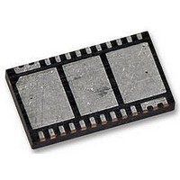
SP7651ER-L Exar Corporation, SP7651ER-L Datasheet - Page 9

SP7651ER-L
Manufacturer Part Number
SP7651ER-L
Description
IC BUCK REG 900KHZ 26DFN
Manufacturer
Exar Corporation
Series
Power Blox™r
Type
Step-Down (Buck)r
Datasheet
1.SP7651ER-LTR.pdf
(15 pages)
Specifications of SP7651ER-L
Internal Switch(s)
Yes
Synchronous Rectifier
Yes
Number Of Outputs
1
Voltage - Output
0.8 V ~ 19 V
Current - Output
3A
Frequency - Switching
900kHz
Voltage - Input
2.5 V ~ 20 V
Operating Temperature
-40°C ~ 85°C
Mounting Type
*
Package / Case
26-VFDFN Exposed Pad
Primary Input Voltage
20V
No. Of Outputs
1
Output Voltage
19V
Output Current
3A
No. Of Pins
26
Operating Temperature Range
-40°C To +85°C
Supply Voltage Range
2.5V To 20V
Mounting Style
SMD/SMT
Lead Free Status / RoHS Status
Lead free / RoHS Compliant
Lead Free Status / RoHS Status
Lead free / RoHS Compliant, Lead free / RoHS Compliant
Available stocks
Company
Part Number
Manufacturer
Quantity
Price
Company:
Part Number:
SP7651ER-L
Manufacturer:
SIPEX
Quantity:
3 500
when tantalum capacitors are used. Tantalum
capacitors are known for catastrophic failure
when exposed to surge current, and input
capacitors are prone to such surge current
when power supplies are connected “live”
to low impedance power sources.
Loop Compensation Design
The open loop gain of the whole system
can be divided into the gain of the error
amplifier, PWM modulator, buck converter
output stage, and feedback resistor divider.
In order to cross over at the selected fre-
quency FCO, the gain of the error amplifier
compensates for the attenuation caused by
the rest of the loop at this frequency. The
goal of loop compensation is to manipulate
loop frequency response such that its gain
crosses over 0db at a slope of -20db/dec.
The first step of compensation design is to
pick the loop crossover frequency.
High crossover frequency is desirable for
fast transient response, but often jeopardizes
the higher than the ESR zero but less than
/5 of the switching frequency. The ESR
zero is contributed by the ESR associated
with the output capacitors and can be de-
termined by:
Rev J: 3/4/07
SP765 Voltage Mode Control Loop with Loop Dynamic
Definitions:
R
R
R
V
(Volts)
ESR
DC
RAMP_PP
REF
= Output Inductor DC Resistance
= Output Capacitor Equivalent Series Resistance
+
_
= SP765 internal RAMP Amplitude Peak-to-Peak Voltage
Notes: R
Condition: Cz2 >> Cp1 & R1 >> Rz3
Output Load Resistance >> R
R
V
ESR
DC
RAMP_PP
SR1Cz2(SRz3Cz3+1)(SRz2Cp1+1)
= Output Inductor DC Resistance.
= Output Capacitor Equivalent Series Resistance.
Type III V oltage Loop
G
= SP6132 Internal RA MP Amplitude Peak to Peak V oltage.
(SRz2Cz2+1)(SR1Cz3+1)
AMP
SP765 Wide Input Voltage Range 3A, 900kHz, Buck Regulator
Compensation
(s) Gain Block
ESR
& R
DC
V
(Volts)
FBK
(R
Voltage Feedback
G
1
R
+ R
FBK
9
2
PWM Stage
G
V
2
Gain Block
RAMP_PP
)
PWM
Block
V
or
system stability. Crossover frequency should
be higher than the ESR zero but less than
/5 of the switching frequency. The ESR
zero is contributed by the ESR associated
with the output capacitors and can be de-
termined by:
The next step is to calculate the complex
conjugate poles contributed by the LC
output filter,
When the output capacitors are Ceramic
type, the SP765 Evaluation Board requires
a Type III compensation circuit to give a phase
boost of 180° in order to counteract the effects
of an underdamped resonance of the output
filter at the double pole frequency.
IN
Gain
V
V
OUT
REF
ƒ
ƒ
z(ESR)
P(LC)
APPLICATIONS INFORMATION
[S^2LC
=
(SR
OUT
=
+S(R
ESR
Output Stage
G
OUT
2π C
2π
C
ESR
Block
OUT
(s) Gain
+R
+ 1)
© Copyright 2007 Sipex Corporation
DC
√
) C
OUT
OUT
L C
+1]
R
OUT
ESR
.
.
V
(Volts)
OUT


