AD7298BCPZ Analog Devices Inc, AD7298BCPZ Datasheet
AD7298BCPZ
Specifications of AD7298BCPZ
Available stocks


Related parts for AD7298BCPZ


AD7298BCPZ Summary of contents
Page 1
FEATURES 12-bit SAR ADC 8 single-ended inputs Channel sequencer functionality Fast throughput of 1 MSPS Analog input range 2.5 V 12-bit temperature-to-digital converter Temperature sensor accuracy of ±1°C Temperature range: −40°C to +125°C Specified for V : ...
Page 2
AD7298 TABLE OF CONTENTS Features .............................................................................................. 1 General Description ......................................................................... 1 Functional Block Diagram .............................................................. 1 Product Highlights ........................................................................... 1 Revision History ............................................................................... 2 Specifications ..................................................................................... 3 Timing Specifications .................................................................. 5 Absolute Maximum Ratings ............................................................ 6 ESD Caution .................................................................................. 6 ...
Page 3
SPECIFICATIONS DRIVE otherwise noted. Table 1. Parameter DYNAMIC PERFORMANCE , 2 Signal-to-Noise Ratio (SNR) 1 Signal-to-Noise (and Distortion) Ratio (SINAD) 1 Total Harmonic Distortion ...
Page 4
AD7298 Parameter LOGIC INPUTS Input High Voltage, V INH Input Low Voltage, V INL Input Current Input Capacitance LOGIC OUTPUTS Output High Voltage Output Low Voltage Floating State Leakage Current 3 ...
Page 5
TIMING SPECIFICATIONS DRIVE initial release to ensure compliance. All input signals are specified with (10% to 90% of ...
Page 6
AD7298 ABSOLUTE MAXIMUM RATINGS Table 3. Parameter V to GND, GND1 GND, GND1 DRIVE Analog Input Voltage to GND1 Digital Input Voltage to GND Digital Output Voltage to GND V to GND1 REF GND1 to GND Input ...
Page 7
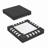
PIN CONFIGURATION AND FUNCTION DESCRIPTION Table 5. Pin Function Descriptions Pin No. Mnemonic Description Analog Inputs. The AD7298 has eight single-ended analog inputs that are multiplexed into the on-chip track- IN3 IN4 18 to ...
Page 8
AD7298 Pin No. Mnemonic Description 16 V Logic Power Supply Input. The voltage supplied at this pin determines at the voltage at which the interface DRIVE operates. This pin should be decoupled to GND. The voltage range on this pin ...
Page 9
TYPICAL PERFORMANCE CHARACTERISTICS –20 f SNR = 72.621 THD = –82.562 –40 –60 –80 –100 –120 0 50 100 150 200 250 300 FREQUENCY (kHz) Figure 3.Typical FFT 1 25° ...
Page 10
AD7298 3 DRIVE 2.5 2.0 1.5 1.0 0 0.5 1.0 1.5 2.0 2.5 CURRENT LOAD (mA) Figure 9. V vs. Reference Output Current Drive REF ...
Page 11
TEMPERATURE (°C) Figure 15. Temperature Accuracy –60 R – 200Ω SOURCE –70 R ...
Page 12
AD7298 TERMINOLOGY Signal-to-Noise and Distortion Ratio (SINAD) The measured ratio of signal-to-noise and distortion at the output of the ADC. The signal is the rms amplitude of the fundamental. Noise is the sum of all nonfundamental signals up to half ...
Page 13
CIRCUIT INFORMATION The AD7298 is a high speed, 8-channel, 12-bit ADC with an internal temperature sensor. The part can be operated from a 2 3.6 V supply and is capable of throughput rates of 1 MSPS per analog ...
Page 14
AD7298 111...111 111...110 111...000 011...111 1LSB = V REF 000...010 000...001 000...000 0V 1LSB +V ANALOG INPUT NOTES 2.5V. REF Figure 23. Straight Binary Transfer Characteristic TEMPERATURE SENSOR OPERATION The AD7298 contains one local temperature sensor. The ...
Page 15
Temperature Value Format One LSB of the ADC corresponds to 0.25°C. The temperature reading from the ADC is stored in a 12-bit twos complement format to accommodate both positive and negative temperature measurements. The temperature data format is provided in ...
Page 16
AD7298 CONTROL REGISTER The control register of the AD7298 is a 16-bit, write-only register. Data is loaded from the DIN pin of the AD7298 on the falling edge of SCLK. The data is transferred on the DIN line at the ...
Page 17
MODES OF OPERATION The AD7298 offers different modes of operation, that are designed to provide additional flexibility for the user. These options can be chosen by programming the content of the control register to select the desired mode. TRADITIONAL MULTICHANNEL ...
Page 18
AD7298 SCLK INVALID DATA DOUT DIN DATA WRITTEN TO CONTROL REGISTER AND CH 2 SELECTED: REPEAT = SCLK CONVERSION RESULT DOUT FOR CHANNEL 1 NO WRITE TO THE DIN CONTROL ...
Page 19
POWER-DOWN MODES The AD7298 has a number of power conservation modes of operation, that are designed to provide flexible power management options. These options can be chosen to optimize the power dissipation/throughput rate ratio for different application requirements. The power-down ...
Page 20
AD7298 Full Power-Down Mode In this mode, all internal circuitry on the AD7298 is powered down and no information is retained in the control register or any other internal register. If the averaging feature for the tempera- ture sensor is ...
Page 21
SERIAL INTERFACE Figure 30 shows the detailed timing diagram for the serial interface to the AD7298. The serial clock provides the conver- sion clock and controls the transfer of information to and from the AD7298 during each conversion. The CS ...
Page 22
AD7298 TEMPERATURE SENSOR READ The temperature sensor conversion involves two phases, the integration phase and the conversion phase as detailed in the Temperature Sensor Operation section. The integration phase is initiated on the falling edge of CS and once completed ...
Page 23
LAYOUT AND CONFIGURATION POWER SUPPLY BYPASSING AND GROUNDING For optimum performance, carefully consider the power supply and ground return layout on any PCB where the AD7298 is used. The PCB containing the AD7298 should have separate analog and digital sections, ...
Page 24
... SEATING PLANE ORDERING GUIDE 1 Model Temperature Range AD7298BCPZ −40°C to +125°C AD7298BCPZ-RL7 −40°C to +125°C EVAL-AD7298SDZ RoHS Compliant Part. ©2010–2011 Analog Devices, Inc. All rights reserved. Trademarks and registered trademarks are the property of their respective owners. 4.10 0.30 4 ...