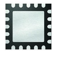
MCP4461T-502E/ML Microchip Technology, MCP4461T-502E/ML Datasheet - Page 45

MCP4461T-502E/ML
Manufacturer Part Number
MCP4461T-502E/ML
Description
IC DGTL POT 257TAPS 5K 20QFN
Manufacturer
Microchip Technology
Datasheet
1.MCP4441-103EML.pdf
(100 pages)
Specifications of MCP4461T-502E/ML
Package / Case
20-VFQFN Exposed Pad
Temperature Coefficient
150 ppm/°C Typical
Taps
257
Resistance (ohms)
5K
Number Of Circuits
4
Memory Type
Non-Volatile
Interface
I²C, 2-Wire Serial
Voltage - Supply
2.7 V ~ 5.5 V
Operating Temperature
-40°C ~ 125°C
Mounting Type
Surface Mount
Number Of Pots
Quad
Taps Per Pot
257
Resistance
5 KOhms
Wiper Memory
Non Volatile
Buffered Wiper
Buffered
Digital Interface
I2C
Operating Supply Voltage
2.7 V to 5.5 V
Supply Current
600 uA
Maximum Operating Temperature
+ 125 C
Minimum Operating Temperature
- 40 C
Description/function
Quad I2C Digital POT with Nonvolatile Memory
Mounting Style
SMD/SMT
Supply Voltage (max)
5.5 V
Supply Voltage (min)
2.7 V
Lead Free Status / RoHS Status
Lead free / RoHS Compliant
REGISTER 4-1:
© 2010 Microchip Technology Inc.
bit 3
bit 2
bit 1
bit 0
Note 1:
Requires a High Voltage command to modify the state of this bit (for Nonvolatile devices only). This bit is
not directly written, but reflects the system state (for this feature).
WL1: WiperLock Status bit for Resistor Network 1 (Refer to
further information)
The WiperLock Technology bit (WL1) prevents the Volatile and Nonvolatile Wiper 1 addresses and the
TCON0 register bits R1HW, R1A, R1W, and R1B from being written to. High Voltage commands are
required to enable and disable WiperLock Technology.
1 = Wiper and TCON0 register bits R1HW, R1A, R1W, and R1B of Resistor Network 1 (Pot 1) are
0 = Wiper and TCON0 of Resistor Network 1 (Pot 1) can be modified
WL0: WiperLock Status bit for Resistor Network 0 (Refer to
further information)
The WiperLock Technology bit (WL0) prevents the Volatile and Nonvolatile Wiper 0 addresses and the
TCON0 register bits R0HW, R0A, R0W, and R0B from being written to. High Voltage commands are
required to enable and disable WiperLock Technology.
1 = Wiper and TCON0 register bits R0HW, R0A, R0W, and R0B of Resistor Network 0 (Pot 0) are
0 = Wiper and TCON0 of Resistor Network 0 (Pot 0) can be modified
Reserved: Forced to “1”
WP: EEPROM Write Protect Status bit (Refer to
information)
This bit indicates the status of the write protection on the EEPROM memory. When Write Protect is
enabled, writes to all nonvolatile memory are prevented. This includes the General Purpose EEPROM
memory, and the nonvolatile Wiper registers. Write Protect does not block modification of the volatile
wiper register values or the volatile TCON0 and TCON1 register values (via Increment, Decrement, or
Write commands).
This status bit is an OR of the devices Write Protect pin (WP) and the internal nonvolatile WP bit. High
Voltage commands are required to enable and disable the internal WP EEPROM bit.
1 = EEPROM memory is Write Protected
0 = EEPROM memory can be written
Note:
Note:
“Locked” (Write Protected)
“Locked” (Write Protected)
STATUS REGISTER (CONTINUED)
The WL1 bit always reflects the result of the last programming cycle to the nonvolatile WL1
bit. After a POR/BOR or RESET pin event, the WL1 bit is loaded with the nonvolatile WL1 bit
value.
The WL0 bit always reflects the result of the last programming cycle to the nonvolatile WL0
bit. After a POR/BOR or RESET pin event, the WL0 bit is loaded with the nonvolatile WL0 bit
value.
Section “EEPROM Write Protect”
Section 5.3 “WiperLock Technology”
Section 5.3 “WiperLock Technology”
MCP444X/446X
DS22265A-page 45
for further
for
for


