MCF51MM256VMB Freescale Semiconductor, MCF51MM256VMB Datasheet - Page 22
MCF51MM256VMB
Manufacturer Part Number
MCF51MM256VMB
Description
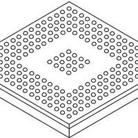
IC MCU 32BIT 256K COLDF 81-PBGA
Manufacturer
Freescale Semiconductor
Series
MCF51MMr
Datasheet
1.TWR-MCF51MM.pdf
(58 pages)
Specifications of MCF51MM256VMB
Core Processor
Coldfire V1
Core Size
32-Bit
Speed
50MHz
Connectivity
CAN, EBI/EMI, I²C, SCI, SPI, USB OTG
Peripherals
LVD, PWM, WDT
Number Of I /o
48
Program Memory Size
256KB (256K x 8)
Program Memory Type
FLASH
Ram Size
32K x 8
Voltage - Supply (vcc/vdd)
1.8 V ~ 3.6 V
Data Converters
A/D 8x16b, D/A 1x12b
Oscillator Type
External
Operating Temperature
-40°C ~ 105°C
Package / Case
81-LBGA
Core
ColdFire V1
Data Bus Width
32 bit
Data Ram Size
32 KB
Interface Type
SCI, SPI, Mini FlexBus
Maximum Clock Frequency
50.3 MHz
Operating Supply Voltage
1.8 V to 3.3 V
Maximum Operating Temperature
+ 105 C
Mounting Style
SMD/SMT
Minimum Operating Temperature
- 40 C
Lead Free Status / RoHS Status
Lead free / RoHS Compliant
Eeprom Size
-
Lead Free Status / Rohs Status
Details
Available stocks
Company
Part Number
Manufacturer
Quantity
Price
Company:

Part Number:
MCF51MM256VMB
Manufacturer:
Freescale Semiconductor
Quantity:
10 000


Electrical Characteristics
22
Freescale reserves the right to change the detail specifications as may be required to permit improvements in the design of its products.
1
2
3
4
5
6
7
8
9
10
11
Num Symbol
20
21
22
23
Typical values are measured at 25C. Characterized, not tested
As the supply voltage rises, the LVD circuit will hold the MCU in reset until the supply has risen above V
Does not include analog module pins. Dedicated analog pins should not be pulled to V
used to reduce current leakage.
Measured with V
All functional non-supply pins are internally clamped to V
Input must be current limited to the value specified. To determine the value of the required current-limiting resistor, calculate
resistance values for positive and negative clamp voltages, then use the larger of the two values.
Power supply must maintain regulation within operating V
If positive injection current (V
supply going out of regulation. Ensure external V
greatest risk when the MCU is not consuming power. Examples are: if no system clock is present, or if clock rate is very low (which
would reduce overall power consumption).
Maximum is highest voltage that POR is guaranteed.
Run at 1 MHz bus frequency
Low voltage detection and warning limits measured at 1 MHz bus frequency.
Factory trimmed at V
V
V
V
V
LVWH
LVWL
hys
BG
Low-voltage
warning
threshold —
high range
Low-voltage
warning
threshold —
low range
Low-voltage inhibit
reset/recoverhysteresis
Bandgap Voltage Reference
In
= V
DD
DD
= 3.0 V, Temp = 25C
.
9
Characteristic
9
In
> V
DD
) is greater than I
Table 9. DC Characteristics (continued)
V
V
V
V
DD
DD
DD
DD
10
falling
rising
falling
rising
11
DD
load will shunt current greater than maximum injection current. This will be the
DD
, the injection current may flow out of V
DD
SS
range during instantaneous and operating maximum current conditions.
and V
Condition
—
—
—
—
—
—
DD
except PTD1.
1.110
2.36
2.36
2.11
2.16
Min
—
DD
or V
SS
DD
Typ
2.46
2.46
2.16
2.21
1.17
and should be left floating when not
50
and could result in external power
1
LVDL
1.230
Max
2.56
2.56
2.22
2.27
—
Freescale Semiconductor
.
Unit
mV
V
V
V
V
V
C
C
P
P
P
P
P
Related parts for MCF51MM256VMB
Image
Part Number
Description
Manufacturer
Datasheet
Request
R

Part Number:
Description:
IC MCU 32BIT 256K FLASH 100LQFP
Manufacturer:
Freescale Semiconductor
Datasheet:

Part Number:
Description:
IC MCU 32BIT 256K FLASH 100LQFP
Manufacturer:
Freescale Semiconductor
Datasheet:

Part Number:
Description:
IC MCU 32BIT 256K FLASH 81MAPBGA
Manufacturer:
Freescale Semiconductor
Datasheet:
Part Number:
Description:
IC MCU 32BIT 256K FLASH 80LQFP
Manufacturer:
Freescale Semiconductor
Datasheet:
Part Number:
Description:
IC MCU 32BIT 256K FLASH 80LQFP
Manufacturer:
Freescale Semiconductor
Datasheet:
Part Number:
Description:
IC MCU 32BIT 256K FLSH 104MAPBGA
Manufacturer:
Freescale Semiconductor
Datasheet:

Part Number:
Description:
IC MCU 32BIT 128K COLDF 80-LQFP
Manufacturer:
Freescale Semiconductor
Datasheet:
Part Number:
Description:
IC MCU 32BIT 128K COLDF 81-LQFP
Manufacturer:
Freescale Semiconductor
Datasheet:

Part Number:
Description:
IC MCU 32BIT 128K COLDF 81-PBGA
Manufacturer:
Freescale Semiconductor
Datasheet:
Part Number:
Description:
IC MCU 32BIT 128K COLDF 81-PBGA
Manufacturer:
Freescale Semiconductor
Datasheet:

Part Number:
Description:
IC MCU 32BIT 256K COLDF 104-PBGA
Manufacturer:
Freescale Semiconductor
Datasheet:

Part Number:
Description:
Manufacturer:
Freescale Semiconductor, Inc
Datasheet:
Part Number:
Description:
Manufacturer:
Freescale Semiconductor, Inc
Datasheet: