GM2BB27BMAC Sharp Microelectronics, GM2BB27BMAC Datasheet - Page 26
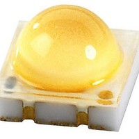
GM2BB27BMAC
Manufacturer Part Number
GM2BB27BMAC
Description
LED High Power (> 0.5 Watts) Double Dome 0.5W White 2700K CCT
Manufacturer
Sharp Microelectronics
Datasheet
1.GM2BB27BMAC.pdf
(27 pages)
Specifications of GM2BB27BMAC
Illumination Color
Warm White
Wavelength/color Temperature
2700 K
Luminous Flux
27 lm
Power Rating
0.5 W
Operating Voltage
3.6 V
Operating Current
140 mA
Minimum Operating Temperature
- 30 C
Maximum Operating Temperature
+ 100 C
Package / Case
2.8 mm x 2.8 mm
Lead Free Status / RoHS Status
Lead free / RoHS Compliant


6.3 洗浄について Cleaning
Moreover, after the reflow process, if the activator remains in the flux between anode and cathode, the remaining
activator might react during high temperature operation, and the electro-migration is generated and there will be a
possibility of a short-circuit. Please use it after confirming the electro-migration is not generated while mounted
actual.
⑤ 推奨パターン
Recommended solder pad design
スクリーン印刷のメタルマスクとしては、0.15mm 厚程度を推奨します。ご使用されるリフロー条件、
はんだペーストおよび基板材質等により、 はんだ付け性が変動することがありますので、 実使用条件に
て十分ご確認の上でご使用下さい。
また、 メタル開口部の間隔やメタル厚みによっては、 フラックス中に活性剤が残留しやすくなることが
あり、LED 端子間でのマイグレーションによるリークが発生する可能性があります。実際の実装状態
で、マイグレーションが発生しないことをご確認後、ご使用下さい。
We recommend the metal mask of thickness 0.15mm for screen-printing. Solderability depends on the reflow
conditions, solder paste, and materials of the PCBs etc. Please test and verify the solderability under the actual solder
method.
Moreover, it might have a risk of short-circuit (leakage) with the electro-migration by the remining activator in the
flux. Please make a suitable selection and test of the metal mask in terms of pitch size and thikness before mass
production.
⑥ リフロー後の全面裏面ディップ
Precautions for PCB backside dip process
設計にてリフロー面の裏面をディップする場合は、 基板裏面側のディップ時の熱及び基板の反り等によ
り、 パッケージ内部の不具合を誘発する恐れがありますので、 御社の製造条件にて、 充分ご確認いただ
いた上、 ご使用下さい。 また、 リフロー終了後はできるだけ速やかに裏面ディップ処理を行って下さい。
できるだけ裏面ディップ実施後、本製品のリフロー処理をお願いします。
Please verify your conditions carefully in giving the dip process on the backside of the PCBs, since the warped
boards caused by heat and heat itself affect the inside of the package. It is recommended to give the reflow process
after dip process. Though it is also available to give the reflow process before the dip process, the interval of the two
processes should be as short as possible.
・ 洗浄によりパッケージ及び樹脂が侵される恐れがございますので、基本的には無洗浄タイプのはんだを使
用し、洗浄は行わないで下さい。
Avoid cleaning the PCBs, since packages and resin are eroded by cleaning. Please use the soldering paste without need of
cleaning.
・ 超音波洗浄は行わないで下さい。
Avoid ultrasonic cleaning.
1.15
2.8
0.25
0.5
Doc. No. DG-101014B Page 24/ 24
Model No. GM2BB27BMAC
(単位 Unit : mm)
Related parts for GM2BB27BMAC
Image
Part Number
Description
Manufacturer
Datasheet
Request
R

Part Number:
Description:
IC FLASH 32MBIT 110NS 56SSOP
Manufacturer:
Sharp Microelectronics
Datasheet:

Part Number:
Description:
IC FLASH 16MBIT 100NS 56TSOP
Manufacturer:
Sharp Microelectronics
Datasheet:

Part Number:
Description:
IC FLASH 64MBIT 120NS 56TSOP
Manufacturer:
Sharp Microelectronics
Datasheet:

Part Number:
Description:
IC FLASH 16MBIT 90NS 48TSOP
Manufacturer:
Sharp Microelectronics
Datasheet:
Part Number:
Description:
IC SRAM 16KBIT 100NS 24DIP
Manufacturer:
Sharp Microelectronics
Datasheet:
Part Number:
Description:
IC SRAM 16KBIT 100NS 24SOP
Manufacturer:
Sharp Microelectronics
Datasheet:
Part Number:
Description:
IC SRAM 64KBIT 100NS 28DIP
Manufacturer:
Sharp Microelectronics
Datasheet:
Part Number:
Description:
IC SRAM 64KBIT 100NS 28SOP
Manufacturer:
Sharp Microelectronics
Datasheet:
Part Number:
Description:
IC SRAM 64KBIT 100NS 28SOP
Manufacturer:
Sharp Microelectronics
Datasheet:
Part Number:
Description:
IC SRAM 256KBIT 70NS 28DIP
Manufacturer:
Sharp Microelectronics
Datasheet:
Part Number:
Description:
IC FLASH 8MBIT 90NS 48TSOP
Manufacturer:
Sharp Microelectronics
Datasheet:
Part Number:
Description:
IC FLASH 8MBIT 85NS 40TSOP
Manufacturer:
Sharp Microelectronics
Datasheet:
Part Number:
Description:
IC FLASH 8MBIT 85NS 40TSOP
Manufacturer:
Sharp Microelectronics
Datasheet:
Part Number:
Description:
IC FLASH 16MBIT 90NS 48TSOP
Manufacturer:
Sharp Microelectronics
Datasheet:
Part Number:
Description:
IC FLASH 16MBIT 70NS 56TSOP
Manufacturer:
Sharp Microelectronics
Datasheet: