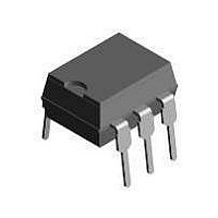
TCDT1122G Vishay, TCDT1122G Datasheet

TCDT1122G
Specifications of TCDT1122G
Available stocks
Related parts for TCDT1122G
TCDT1122G Summary of contents
Page 1
... CTR > DIP-6 TCDT1122 CTR 63 - 125 %, DIP-6 TCDT1123 CTR 100 - 200 %, DIP-6 TCDT1124 CTR 160 - 320 %, DIP-6 TCDT1120G CTR > DIP-6 TCDT1122G CTR 63 - 125 %, DIP-6 TCDT1123G CTR 100 - 200 %, DIP-6 TCDT1124G CTR 160 - 320 %, DIP Leadform 10.16 mm not marked on the body e3 Pb Pb-free www ...
Page 2
... TCDT1120/ TCDT1120G Vishay Semiconductors Absolute Maximum Ratings °C, unless otherwise specified amb Stresses in excess of the absolute Maximum Ratings can cause permanent damage to the device. Functional operation of the device is not implied at these or any other conditions in excess of those given in the operational sections of this document. Exposure to absolute Maximum Rating for extended periods of the time can adversely affect reliability ...
Page 3
... CEsat = 10 mA Test condition Part = 1 mA TCDT1120 F TCDT1120G TCDT1122 TCDT1122G TCDT1123 TCDT1123G TCDT1124 TCDT1124G = 10 mA TCDT1120 F TCDT1120G TCDT1122 TCDT1122G TCDT1123 TCDT1123G TCDT1124 TCDT1124G Test condition Symbol I F Test condition Symbol P diss Vishay Semiconductors Min Typ. Max 150 Min Typ. Max 0.3 110 0 ...
Page 4
... TCDT1120/ TCDT1120G Vishay Semiconductors Coupler Parameter Rated impulse voltage Safety temperature Insulation Rated Parameters Parameter Partial discharge test voltage - 100 %, t Routine test Partial discharge test voltage - Lot test (sample test) (see figure 2) Insulation resistance V = 500 500 500 (construction test only) 300 ...
Page 5
... Figure 6. Relative Current Transfer Ratio vs. Ambient 10000 1000 100 120 95 11038 Figure 7. Collector Dark Current vs. Ambient Temperature 100 0.1 0.01 0.1 95 11040 Figure 8. Collector Current vs. Forward Current Vishay Semiconductors =5V CE =10mA T – Ambient Temperature (°C ) amb Temperature V =30V 100 – Ambient Temperature ( °C ) ...
Page 6
... TCDT1120/ TCDT1120G Vishay Semiconductors 100 I =50mA CNY75A 0.1 0 – Collector Emitter Voltage ( 11041 CE Figure 9. Collector Current vs. Collector Emitter Voltage 1.0 CTR=50% 0.8 CNY75A 0.6 0.4 20% 0.2 10 – Collector Current ( 11034 C Figure 10. Collector Emitter Saturation Voltage vs. Collector Current 1000 TCDT1122(G) V =5V CE 100 ...
Page 7
... Rev. 1.6, 26-Oct-04 TCDT1120/ TCDT1120G off 14803 Figure 18. Turn on / off Time vs. Collector Current 20 t off 14804 Figure 19. Turn on / off Time vs. Collector Current 10 Vishay Semiconductors TCDT1123(G) Non Saturated Operation V =5V S =100 Ω off – Collector Current ( TCDT1124(G) Non Saturated Operation V =5V S =100 Ω ...
Page 8
... TCDT1120/ TCDT1120G Vishay Semiconductors Package Dimensions in mm Package Dimensions in mm www.vishay.com 8 14771 Document Number 83532 Rev. 1.6, 26-Oct-04 ...
Page 9
... Various national and international initiatives are pressing for an earlier ban on these substances. Vishay Semiconductor GmbH has been able to use its policy of continuous improvements to eliminate the use of ODSs listed in the following documents. 1. Annex A, B and list of transitional substances of the Montreal Protocol and the London Amendments respectively 2 ...
Page 10
... Information contained herein is intended to provide a product description only. No license, express or implied, by estoppel or otherwise, to any intellectual property rights is granted by this document. Except as provided in Vishay's terms and conditions of sale for such products, Vishay assumes no liability whatsoever, and disclaims any express or implied warranty, relating to sale and/or use of Vishay products including liability or warranties relating to fitness for a particular purpose, merchantability, or infringement of any patent, copyright, or other intellectual property right ...


