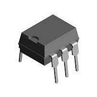
TCDT1110 Vishay, TCDT1110 Datasheet - Page 2

TCDT1110
Manufacturer Part Number
TCDT1110
Description
Transistor Output Optocouplers Phototransistor Out Single CTR > 100%
Manufacturer
Vishay
Specifications of TCDT1110
Isolation Voltage
3750 Vrms
Maximum Input Diode Current
60 mA
Maximum Reverse Diode Voltage
6 V
Output Device
Transistor
Output Type
DC
Configuration
1
Input Type
DC
Maximum Collector Emitter Voltage
70 V
Maximum Collector Emitter Saturation Voltage
300 mV
Maximum Forward Diode Voltage
1.5 V
Maximum Collector Current
50 mA
Maximum Power Dissipation
250 mW
Maximum Operating Temperature
+ 100 C
Minimum Operating Temperature
- 55 C
Package / Case
PDIP-6
No. Of Channels
1
Optocoupler Output Type
Phototransistor
Input Current
50mA
Output Voltage
70V
Opto Case Style
DIP
No. Of Pins
6
Input Current Max
50mA
Approval Bodies
UL
Rohs Compliant
Yes
Lead Free Status / RoHS Status
Lead free / RoHS Compliant
Lead Free Status / RoHS Status
Lead free / RoHS Compliant, Lead free / RoHS Compliant
Available stocks
Company
Part Number
Manufacturer
Quantity
Price
Company:
Part Number:
TCDT1110
Manufacturer:
OKI
Quantity:
6 220
TCDT1110/TCDT1110G
Vishay Semiconductors
Notes
(1)
(2)
Note
T
Minimum and maximum values are testing requirements. Typical values are characteristics of the device and are the result of engineering
evaluation. Typical values are for information only and are not part of the testing requirements.
Note
According to DIN EN 60747-5-5 see figure 1. This optocoupler is suitable for safe electrical isolation only within the safety ratings. Compliance
with the safety ratings shall be ensured by means of suitable protective circuits.
www.vishay.com
784
amb
ABSOLUTE MAXIMUM RATINGS
PARAMETER
OUTPUT
Collector emitter voltage
Emitter collector voltage
Collector current
Collector peak current
Power dissipation
Junction temperature
COUPLER
Isolation test voltage (RMS)
Total power dissipation
Ambient temperature range
Storage temperature range
Soldering temperature
ELECTRICAL CHARACTERISTICS
PARAMETER
INPUT
Forward voltage
Junction capacitance
OUTPUT
Collector emitter voltage
Emitter collector voltage
Collector-emitter cut-off current
COUPLER
Collector emitter saturation voltage
Cut-off frequency
Coupling capacitance
CURRENT TRANSFER RATIO
PARAMETER
I
MAXIMUM SAFETY RATINGS
PARAMETER
INPUT
Forward current
OUTPUT
Power dissipation
COUPLER
Rated impulse voltage
Safety temperature
C
T
Functional operation of the device is not implied at these or any other conditions in excess of those given in the operational sections of this
document. Exposure to absolute maximum ratings for extended periods of the time can adversely affect reliability.
Refer to wave profile for soldering conditions for through hole devices.
/I
amb
F
= 25 °C unless otherwise specified.
= 25 °C unless otherwise specified. Stresses in excess of the absolute maximum ratings can cause permanent damage to the device.
(2)
For technical questions, contact: optocoupler.answers@vishay.com
V
2 mm from case t ≤ 10 s
CE
t
p
TEST CONDITION
I
V
/T = 0.5, t
= 5 V, I
F
CE
TEST CONDITION
TEST CONDITION
TEST CONDITION
= 10 mA, I
V
V
Optocoupler, Phototransistor
CE
R
= 20 V, I
t = 1 min
(1)
I
I
= 0, f = 1 MHz
E
F
I
f = 1 MHz
= 30 V, I
C
F
= 100 µA
= 50 mA
= 10 mA, R
= 1 mA
p
≤ 10 ms
C
F
= 0.5 mA
= 10 mA
F
= 0
Output
L
= 1 Ω
SYMBOL
SYMBOL
SYMBOL
SYMBOL
V
V
V
V
T
V
V
P
V
P
T
I
P
T
CTR
I
IOTM
T
CEO
CEsat
CEO
ECO
CM
V
I
T
amb
CEO
ECO
C
I
diss
ISO
C
diss
f
stg
sld
C
tot
F
c
si
j
F
k
j
MIN.
MIN.
MIN.
70
100
7
- 55 to + 100
- 55 to + 125
VALUE
5300
100
150
125
250
260
70
50
7
TYP.
TYP.
TYP.
110
1.2
0.3
50
Document Number: 83531
MAX.
MAX.
MAX.
130
265
150
150
1.5
0.3
6
Rev. 1.8, 16-May-08
UNIT
V
mW
mw
mA
mA
°C
°C
°C
°C
RMS
V
V
UNIT
UNIT
UNIT
mW
kHz
mA
pF
nA
pF
kV
°C
V
V
V
V
%


