VNCLO-MB1A FTDI, VNCLO-MB1A Datasheet - Page 15
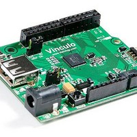
VNCLO-MB1A
Manufacturer Part Number
VNCLO-MB1A
Description
Interface Modules & Development Tools Vinculo Motherboard Req VNC2DEBUGMODULE
Manufacturer
FTDI
Datasheet
1.VNCLO-MB1A.pdf
(26 pages)
Specifications of VNCLO-MB1A
Interface Type
USB, Serial, UART, FIFO, SPI
Data Bus Width
Serial, 8 bit
Operating Supply Voltage
9 V to 12 V
Product
Interface Development Tools
Features
Precompiled Drivers For A Variety Of Interfaces
Kit Contents
Board
Kit Features
Precompiled Drivers, Compatible With Existing Shields
Mcu Supported Families
VNC2
Silicon Family Name
Vinculum
For Use With/related Products
VNC2
Lead Free Status / RoHS Status
Lead free / RoHS Compliant
Other names
VINCULO


4.3 Parallel FIFO Interface - Asynchronous Mode
The Parallel FIFO Asynchronous mode is functionally the same as the Parallel FIFO Interface available in
the FTDI VDIP1 module and has an eight bit data bus, individual read and write strobes and two
hardware flow control signals.
4.3.1 Signal Description - Parallel FIFO Interface
The Parallel FIFO Interface signals can be programmed to a choice of available I/O pins. Table 4.4 shows
the Parallel FIFO Interface signals and the pins that they can be mapped. Details of the operation and
timing can be found in the VNC2 datasheet.
J2-1, J2-5, J3-2, J3-5, J4-6, J5-7, J6-1,
J6-5
J2-2, J2-6, J3-1, J3-6, J4-4, J5-1, J5-4,
J5-8, J6-2, J6-6
J1-1, J2-3, J3-3, J3-7, J4-1, J4-5, J5-2,
J5-5, J6-3, J6-7
J1-2, J2-4, J3-4, J3-8, J4-2, J4-3, J5-3,
J5-6, J6-4, J6-8
J2-1, J2-5, J3-2, J3-5, J4-6, J5-7, J6-1,
J6-5
J2-2, J2-6, J3-1, J3-6, J4-4, J5-1, J5-4,
J5-8, J6-2, J6-6
J1-1, J2-3, J3-3, J3-7, J4-1, J4-5, J5-2,
J5-5, J6-3, J6-7
J1-2, J2-4, J3-4, J3-8, J4-2, J4-3, J5-3,
J5-6, J6-4, J6-8
J2-1, J2-5, J3-2, J3-5, J4-6, J5-7, J6-1,
J6-5
J2-2, J2-6, J3-1, J3-6, J4-4, J5-1, J5-4,
J5-8, J6-2, J6-6
J1-1, J2-3, J3-3, J3-7, J4-1, J4-5, J5-2,
J5-5, J6-3, J6-7
J1-2, J2-4, J3-4, J3-8, J4-2, J4-3, J5-3,
J5-6, J6-4, J6-8
Table 4.4 – Data and Control Bus Signal Mode Options – Parallel FIFO Interface
Note:
1. # defines active low signals.
2. Also PWM outputs can be routed to any of the pins listed in table 4.1
Available Pins
Copyright © 2010-2011 Future Technology Devices International Limited
fifo_data[0]
fifo_data[1]
fifo_data[2]
fifo_data[3]
fifo_data[4]
fifo_data[5]
fifo_data[6]
fifo_data[7]
fifo_txe#
fifo_rxf#
fifo_wr#
fifo_rd#
Name
Vinco Development Module Datasheet Version 2.0
Output
Output
Type
Input
Input
I/O
I/O
I/O
I/O
I/O
I/O
I/O
I/O
Document Reference No.: FT_000327
When high, do not read data from the FIFO.
When low, there is data available in the FIFO
which can be read by strobing RD# low, then
high.
When high, do not write data into the FIFO.
When low, data can be written into the FIFO
by strobing WR high, then low.
Enables the current FIFO data byte on
D0...D7 when low. Fetches the next FIFO
data byte (if available) from the receive FIFO
buffer when RD# goes from high to low
Writes the data byte on the D0...D7 pins into
the transmit FIFO buffer when WR goes from
high to low.
Clearance No.: FTDI#173
FIFO data bus Bit 0
FIFO data bus Bit 1
FIFO data bus Bit 2
FIFO data bus Bit 3
FIFO data bus Bit 4
FIFO data bus Bit 5
FIFO data bus Bit 6
FIFO data bus Bit 7
Description
11
Related parts for VNCLO-MB1A
Image
Part Number
Description
Manufacturer
Datasheet
Request
R

Part Number:
Description:
POWER SUPPLY FOR VNCLO-MB1A USA
Manufacturer:
FTDI, Future Technology Devices International Ltd
Datasheet:

Part Number:
Description:
POWER SUPPLY FOR VNCLO-MB1A EU
Manufacturer:
FTDI, Future Technology Devices International Ltd
Datasheet:
Part Number:
Description:
POWER SUPPLY FOR VNCLO-MB1A UK
Manufacturer:
FTDI, Future Technology Devices International Ltd
Datasheet:

Part Number:
Description:
Interface Modules & Development Tools Vinculo Prototyping Shield Accessory
Manufacturer:
FTDI
Datasheet:
Part Number:
Description:
KIT, DEV, VINCULUM-II, VNC2
Manufacturer:
FTDI
Datasheet:
Part Number:
Description:
BOARD, EVALUATION, US PSU
Manufacturer:
FTDI
Datasheet:
Part Number:
Description:
Specifications: Manufacturer: FTDI ; Product Category: USB Interface IC ; RoHS: Details ; Operating Supply Voltage: 3 V to 5.25 V ; Supply Current: 25 mA ; Maximum Operating Temperature: + 70 C ; Mounting Style: SMD/SMT ; Package / Case: QFN-32
Manufacturer:
FTDI

Part Number:
Description:
IC USB TO SERIAL UART 32-QFN
Manufacturer:
FTDI, Future Technology Devices International Ltd

Part Number:
Description:
USB Interface IC USB to Serial UART Enhanced IC SSOP-28
Manufacturer:
FTDI
Datasheet:

Part Number:
Description:
IC, USB UART INTERFACE, SSOP-28
Manufacturer:
FTDI
Datasheet:

Part Number:
Description:
IC, USB UART INTERFACE, QFN-32
Manufacturer:
FTDI
Datasheet:
Part Number:
Description:
IC, USB FIFO INTERFACE, SSOP-28
Manufacturer:
FTDI
Datasheet:
Part Number:
Description:
MODULE, USB, 4 PORT, FT4232H BASED
Manufacturer:
FTDI
Datasheet:
Part Number:
Description:
357-036-542-201 CARDEDGE 36POS DL .156 BLK LOPRO
Manufacturer:
FTDI
Datasheet:
Part Number:
Description:
357-036-542-201 CARDEDGE 36POS DL .156 BLK LOPRO
Manufacturer:
FTDI
Datasheet: