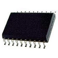
KX1400EW Keterex, KX1400EW Datasheet - Page 18

KX1400EW
Manufacturer Part Number
KX1400EW
Description
Audio D/A Converter ICs KX1400 Audio Playback IC
Manufacturer
Keterex
Datasheet
1.KX1400EW.pdf
(29 pages)
Specifications of KX1400EW
Resolution
12 bit
Operating Supply Voltage
2.7 V to 5.5 V
Operating Temperature Range
- 40 C to + 85 C
Maximum Power Dissipation
120 mW
Mounting Style
SMD/SMT
Number Of Dac Outputs
2
Power Consumption
320 mW
Supply Current
50 mA
Thd Plus Noise
40 dB
Package / Case
SOIC-20
Lead Free Status / RoHS Status
Lead free / RoHS Compliant
as open-drain or push-pull. Refer to Section 8.9 for detailed information on use of the Set Outputs
command. After device reset, all outputs are set to logic level low with push-pull drive characteristics.
and command processing is halted, the speaker driver is disabled and the internal oscillator is stopped.
Power consumption is reduced to about 1 µA (excluding load current sourced by the GPO1/2 outputs).
KX1400 Audio Playback IC
SYMBOL
fosc
Δf
6.10. General Purpose Clock Output
The KX1400 provides a Clock Output feature with the ability to divide the frequency of the internal
precision oscillator and route this signal to the CLKOUT pin. This signal may be used as a time base by
other components in the system. (Note: it is not required to use this signal to synchronize the MCU with
the KX1400. The MCU interface may operate asynchronously to the internal system clock used by the
audio processor, including while streaming audio data to the KX1400 from a host MCU.)
The divisor used to divide the 8.2 MHz internal system clock before the signal is output on the CLKOUT
pin is configured by sending a Set Clock command via the MCU host interface or as part of a phrase
processed from external memory. Table 6.7 shows the possible Clock Divisor values and corresponding
frequencies output on the CLKOUT pin.
The Clock Output feature is enabled by default after a device reset with the Clock Divisor set to divide by
8 (1.025 MHz CLKOUT signal). It may be disabled with the CLKOUT pin forced to the desired steady
state level using the Set Clock command. Refer to Section 8.12 for detailed information on the use of the
Set Clock command. Internal hardware synchronizes execution of the Set Clock command to ensure
minimum pulse width specifications are maintained when changing the Clock Divisor or disabling/enabling
the Clock Output feature.
6.11. General Purpose Digital Outputs
The KX1400 provides two general purpose digital outputs mapped to the GPO1 and GPO2 pins. The
state of these pins is controlled by issuing the Set Outputs command via the host MCU interface or as
part of a phrase processed from external memory. The output drivers for these pins may be configured
6.12. Stand-by Mode
A low-power Stand-by mode is available via an option of the Stop command. In Stand-by mode, all audio
18
OSC
Internal Oscillator Frequency
Internal Oscillator Frequency
Variation
PARAMETER
Table 6.6. Internal Oscillator Electrical Specifications
Table 6.7. Clock Divisor and Output Frequencies
DIVISOR
CLOCK
0
1
2
3
CLOCK DIVIDED BY:
8.2 MHz INTERNAL
VDD = 3.3V, T = 25°C
1
2
4
8
2.7V ≤ VDD ≤ 3.6V
2.7V ≤ VDD ≤ 5.5V
CONDITION
FREQUENCY
1.025 MHz
2.05 MHz
CLKOUT
8.2 MHz
4.1 MHz
8.07
Min
-1
-1
8.192
Typ
Max
8.32
+1
+3
Units
MHz
%
%


