VN2224N3-G Supertex, VN2224N3-G Datasheet

MOSFET Small Signal 240V 1.25Ohm

VN2224N3-G

Manufacturer Part Number
VN2224N3-G
Description
MOSFET Small Signal 240V 1.25Ohm
Manufacturer
Supertex
Datasheet

Specifications of VN2224N3-G

Minimum Operating Temperature
- 55 C
Configuration
Single
Transistor Polarity
N-Channel
Resistance Drain-source Rds (on)
1.25 Ohm @ 10 V
Drain-source Breakdown Voltage
240 V
Gate-source Breakdown Voltage
+/- 20 V
Continuous Drain Current
0.54 A
Power Dissipation
1000 mW
Maximum Operating Temperature
+ 150 C
Mounting Style
Through Hole
Package / Case
TO-92
Lead Free Status / RoHS Status
Lead free / RoHS Compliant
Ordering Information
High Reliability Devices
See pages 5-4 and 5-5 for MILITARY STANDARD Process
Flows and Ordering Information.
11/12/01
Supertex Inc. does not recommend the use of its products in life support applications and will not knowingly sell its products for use in such applications unless it receives an adequate "products liability
indemnification insurance agreement." Supertex does not assume responsibility for use of devices described and limits its liability to the replacement of devices determined to be defective due to
workmanship. No responsibility is assumed for possible omissions or inaccuracies. Circuitry and specifications are subject to change without notice. For the latest product specifications, refer to the
Supertex website: http://www.supertex.com. For complete liability information on all Supertex products, refer to the most current databook or to the Legal/Disclaimer page on the Supertex website.
Features
Applications
Absolute Maximum Ratings
Drain-to-Source Voltage
Drain-to-Gate Voltage
Gate-to-Source Voltage
Operating and Storage Temperature
Soldering Temperature*
* Distance of 1.6 mm from case for 10 seconds.
Free from secondary breakdown
Low power drive requirement
Ease of paralleling
Low C
Excellent thermal stability
Integral Source-Drain diode
High input impedance and high gain
Motor controls
Converters
Amplifiers
Switches
Power supply circuits
Drivers (relays, hammers, solenoids, lamps,
memories, displays, bipolar transistors, etc.)
BV
BV
220V
240V
DSS
DGS
ISS
/
and fast switching speeds
R
1.25Ω
1.25Ω
(max)
DS(ON)
N-Channel Enhancement-Mode
Vertical DMOS FETs
(min)
I
5.0A
5.0A
D(ON)
-55°C to +150°C
BV
300°C
BV
± 20V
DGS
DSS
VN2224N3
Order Number / Package
TO-92
1
Package Options
Advanced DMOS Technology
These enhancement-mode (normally-off) transistors utilize a
vertical DMOS structure and Supertex’s well-proven silicon-gate
manufacturing process. This combination produces devices with
the power handling capabilities of bipolar transistors and with the
high input impedance and positive temperature coefficient inher-
ent in MOS devices. Characteristic of all MOS structures, these
devices are free from thermal runaway and thermally-induced
secondary breakdown.
Supertex’s vertical DMOS FETs are ideally suited to a wide range
of switching and amplifying applications where high breakdown
voltage, high input impedance, low input capacitance, and fast
switching speeds are desired.
Note: See Package Outline section for dimensions.
20-Pin C-Dip
VN2222NC
TO-92
S G D
G1
G2
G3
G4
S
S
S
S
S
S
10
20-pin Ceramic DIP
1
2
3
4
5
6
7
8
9
top view
VN2222
VN2224
20
19
18
17
16
15
14
13
12
11
S
S
NC
D1
D2
D3
D4
NC
S
S

Related parts for VN2224N3-G

VN2224N3-G Summary of contents

Page 1

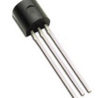
... TO-92 20-Pin C-Dip 5.0A — VN2222NC 5.0A VN2224N3 — Advanced DMOS Technology These enhancement-mode (normally-off) transistors utilize a vertical DMOS structure and Supertex’s well-proven silicon-gate manufacturing process. This combination produces devices with the power handling capabilities of bipolar transistors and with the high input impedance and positive temperature coefficient inher- ent in MOS devices ...

Page 2

Thermal Characteristics Package I (continuous)* D TO-92 540mA * I (continuous) is limited by max rated Electrical Characteristics Symbol Parameter BV Drain-to-Source DSS Breakdown Voltage V Gate Threshold Voltage GS(th) ∆V Change in V with Temperature ...

Page 3

Typical Performance Curves Output Characteristics 10V (volts) DS Transconductance vs. Drain Current 25V - ...

Page 4

... Variation with Temperature DSS 1.1 1.0 0.9 - (°C) j Transfer Characteristics 25V (volts) GS Capacitance vs. Drain-to-Source Voltage 400 f = 1MHz 300 200 100 (volts) DS ©2001 Supertex Inc. All rights reserved. Unauthorized use or reproduction prohibited. 100 150 1.4 1.2 1.0 0.8 0 ISS C RSS On-Resistance vs. Drain Current 10V ...

Related keywords