IES5505D Hendon Semiconductors, IES5505D Datasheet
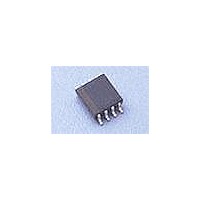
Buffers & Line Drivers 2.7-5.5V Simple 2 Wire Buffer

IES5505D

Manufacturer Part Number
IES5505D
Description
Buffers & Line Drivers 2.7-5.5V Simple 2 Wire Buffer
Manufacturer
Hendon Semiconductors
Datasheet

Specifications of IES5505D

Logic Family
IE5505
Supply Voltage (max)
5.5 V
Supply Voltage (min)
2.7 V
Maximum Operating Temperature
85 C
Mounting Style
SMD/SMT
Minimum Operating Temperature
- 40 C
Supply Current
4 mA
Logic Type
Simple 2 Wire Bus Buffer
Package / Case
MSOP-8L
Lead Free Status / RoHS Status
Lead free / RoHS Compliant
1
• Simple impedance isolating buffer for 2-wire buses
• 30mA (IES5515) or 4mA (IES5505) maximum static
• Works with I
• Fast switching times allow operation in excess of 1MHz
• Enable allows bus segments to be disconnected
• Hysteresis on inputs provides noise immunity
• Operating voltages from 2.7 V to 5.5 V
• Very low supply current
• Uncomplicated characteristics suitable for quick
2
(1) I
© 2008 Hendon Semiconductors Pty. Ltd. , all rights reserved.
2008 Feb 26, Revision 0.7
pull-down capability supports a wide range of bus
standards
mode plus Fm+ (IES5515), SMBus (standard and high
power mode), and PMbus
implementation in most common 2-wire bus applications
Enable
SDA
SCL
Direction
FEATURES
BLOCK DIAGRAM
2
C-bus is a trademark of NXP B.V.
R
1
SDA
SCL
R
DIR
2
2
EN
C
IN
IN
1
6
3
5
(1)
Fig.1 Block diagram
bus Standard mode, Fast mode, Fast
2.7 - 5.5V
8
4
V
GND
DD
IES5505
IES5515
SDA
7
SCL
2
OUT
OUT
R
3
SDA
SCL
R
4
1
3
The IES5505 and IES5515 are monolithic CMOS
integrated circuits for bus buffering in applications
including I
based on similar principles.
The buffer extends the bus load limit by buffering both the
SCL and SDA lines, allowing the maximum permissible
bus capacitance on both sides of the buffer.
The IES5505/15 includes a uni-directional buffer for the
clock signal, and a bi-directional buffer for the data signal.
Slave devices which employ clock stretching are therefore
not supported.
In its most basic implementation, the buffer will allow an
extended number of Slave devices to be attached to one
(or more) Master devices. In this case, all Master devices
would be positioned on the Sxx
The Direction pin further enhances this function by
allowing the uni-directional clock signal to be reversed,
thus allowing Master devices on both sides of the buffer.
The Enable function allows sections of the bus to be
isolated. Individual parts of the system can be brought
on-line sucessively. This means a controlled start-up using
a diverse range of components, operating speeds and
loads is easily achieved.
4
• Electronic Signs & Displays
• Lighting Control (incl. Architectural & Stage lighting)
• Game Consoles / Boxes
• Gaming Machine Networks
• Building Automation
• TV / Projector / Monitor interconnection (DDC)
• Power Management Systems
• Desktop and Portable Computers
• Security Systems
• Interfacing standard 3mA I
GENERAL DESCRIPTION
APPLICATIONS
2
IES5505
C, SMBus, DDC, PMbus, and other systems
Simple 2-Wire Bus Buffer
Contents are subject to the Disclaimer
2
C parts to a 30mA Fm+ bus
Preliminary Specification
IN
side of the IES5505/15.
IES5515

Related parts for IES5505D

IES5505D Summary of contents

Page 1

... GND Fig.1 Block diagram 2 (1) I C-bus is a trademark of NXP B.V. © 2008 Hendon Semiconductors Pty. Ltd. , all rights reserved. 2008 Feb 26, Revision 0.7 3 GENERAL DESCRIPTION The IES5505 and IES5515 are monolithic CMOS integrated circuits for bus buffering in applications including I based on similar principles. ...

Page 2

PINNING INFORMATION 5.1 Pinning layout SCL OUT IES5505 3 SCL IN IES5515 4 GND Fig.2 Pinning diagram (SO8 / MSOP8) 6 FUNCTIONAL DESCRIPTION 6 GND - DC supply pins DD The power supply voltage ...

Page 3

... IES5515 D MSOP-8L micro small outline package; 8 leads; body width 3.0 mm Other package options are available - contact Hendon Semiconductors for details. For more information on packages, please refer to the document “Integrated Circuit Packaging and Soldering Information” on the Hendon Semiconductors web site. 8 ESD CAUTION Electrostatic Discharge (ESD) sensitive device ...

Page 4

... Exposure to limiting values for extended periods may affect device reliability. Application information Where application information is given advisory and does not form part of the specification. 11 COMPANY INFORMATION HENDON SEMICONDUCTORS PTY. LTD. ABN 17 080 879 616 Postal address: Hendon Semiconductors PO Box 2226 ...

Page 5

... DISCLAIMER Hendon Semiconductors Pty. Ltd. ABN 17 080 879 616 (“Hendon”) reserves the right to make changes to both its products and product data without notice. Hendon makes no warranty, representation or guarantee regarding the suitability of its products for any particular purpose, nor does Hendon assume any liability arising out of the use or application of any Hendon product. Hendon specifically disclaims any and all liability, including without limitation incidental or consequential damages ...

Related keywords