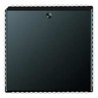
PIC18F6680-I/L Microchip Technology, PIC18F6680-I/L Datasheet - Page 98

PIC18F6680-I/L
Manufacturer Part Number
PIC18F6680-I/L
Description
Microcontrollers (MCU) 64KB 3328 RAM 52 I/O
Manufacturer
Microchip Technology
Datasheet
1.PCM18XK1.pdf
(496 pages)
Specifications of PIC18F6680-I/L
Processor Series
PIC18F
Core
PIC
Data Bus Width
8 bit
Data Ram Size
3.25 KB
Interface Type
I2C/SPI/AUSART/CAN
Maximum Clock Frequency
40 MHz
Number Of Programmable I/os
53
Number Of Timers
5
Operating Supply Voltage
4.2 V to 5.5 V
Maximum Operating Temperature
+ 85 C
Mounting Style
SMD/SMT
3rd Party Development Tools
52715-96, 52716-328, 52717-734, 52712-325, EWPIC18
Development Tools By Supplier
PG164130, DV164035, DV244005, DV164005, PG164120, ICE2000, ICE4000, DV164136
Minimum Operating Temperature
- 40 C
On-chip Adc
12-ch x 10-bit
Program Memory Type
Flash
Program Memory Size
64 KB
Package / Case
PLCC-68
Lead Free Status / RoHS Status
Lead free / RoHS Compliant
Available stocks
Company
Part Number
Manufacturer
Quantity
Price
Company:
Part Number:
PIC18F6680-I/L
Manufacturer:
RUBYCON
Quantity:
46 000
Part Number:
PIC18F6680-I/L
Manufacturer:
MICROCH
Quantity:
20 000
- Current page: 98 of 496
- Download datasheet (9Mb)
PIC18F6585/8585/6680/8680
6.2
The external memory interface implemented in
PIC18F8X8X devices operates only in 16-bit mode.
The mode selection is not software configurable but is
programmed via the configuration bits.
The WM<1:0> bits in the MEMCON register determine
three types of connections in 16-bit mode. They are
referred to as:
• 16-bit Byte Write
• 16-bit Word Write
• 16-bit Byte Select
These three different configurations allow the designer
maximum flexibility in using 8-bit and 16-bit memory
devices.
FIGURE 6-1:
DS30491C-page 96
Note 1: This signal only applies to table writes. See Section 5.1 “Table Reads and Table Writes”.
PIC18F8X8X
16-bit Mode
AD<15:8>
A<19:16>
AD<7:0>
WRH
WRL
ALE
OE
CE
16-BIT BYTE WRITE MODE EXAMPLE
373
373
D<7:0>
A<19:0>
D<15:8>
For all 16-bit modes, the Address Latch Enable (ALE)
pin indicates that the Address bits (A<15:0>) are avail-
able on the external memory interface bus. Following
the address latch, the Output Enable signal (OE ) will
enable both bytes of program memory at once to form
a 16-bit instruction word.
In Byte Select mode, JEDEC standard Flash memories
will require BA0 for the byte address line, and one I/O
line to select between Byte and Word mode. The other
16-bit modes do not need BA0. JEDEC standard static
RAM memories will use the UB or LB signals for byte
selection.
6.2.1
Figure 6-1 shows an example of 16-bit Byte Write
mode for PIC18F8X8X devices.
16-BIT BYTE WRITE MODE
A<x:0>
D<7:0>
CE
OE
(MSB)
WR
(1)
2004 Microchip Technology Inc.
Address Bus
Data Bus
Control Lines
D<7:0>
A<x:0>
D<7:0>
CE
OE
(LSB)
WR
(1)
Related parts for PIC18F6680-I/L
Image
Part Number
Description
Manufacturer
Datasheet
Request
R

Part Number:
Description:
20-Pin USB Flash Microcontrollers
Manufacturer:
MICROCHIP [Microchip Technology]
Datasheet:

Part Number:
Description:
PIC18F With 128-segment LCD Driver And 12-bit ADC, 8KB Flash, 768B RAM, CCP, MSS
Manufacturer:
Microchip Technology
Datasheet:

Part Number:
Description:
PIC18F With 128-segment LCD Driver And 12-bit ADC, 16KB Flash, 768B RAM, CCP, MS
Manufacturer:
Microchip Technology
Datasheet:

Part Number:
Description:
PIC18F With 192-segment LCD Driver And 12-bit ADC, 8KB Flash, 768B RAM, CCP, MSS
Manufacturer:
Microchip Technology
Datasheet:

Part Number:
Description:
PIC18F With 192-segment LCD Driver And 12-bit ADC, 16KB Flash, 768B RAM, CCP, MS
Manufacturer:
Microchip Technology
Datasheet:

Part Number:
Description:
Microcontrollers (MCU) 48KB 3328 RAM 52 I/O
Manufacturer:
Microchip Technology
Datasheet:

Part Number:
Description:
32kB Flash, 2kB RAM, 1kB EE, NanoWatt XLP, LCD 64 QFN 9x9x0.9mm T/R
Manufacturer:
Microchip Technology
Datasheet:

Part Number:
Description:
32kB Flash, 2kB RAM, 1kB EE, NanoWatt XLP, LCD 64 TQFP 10x10x1mm T/R
Manufacturer:
Microchip Technology
Datasheet:

Part Number:
Description:
128kB Flash, 4kB RAM, 1kB EE, 16MIPS, NanoWatt XLP, LCD, 5V 80 TQFP 12x12x1mm T/
Manufacturer:
Microchip Technology
Datasheet:

Part Number:
Description:
32kB Flash, 2kB RAM, 1kB EE, NanoWatt XLP, LCD 64 QFN 9x9x0.9mm TUBE
Manufacturer:
Microchip Technology
Datasheet:

Part Number:
Description:
32kB Flash, 2kB RAM, 1kB EE, NanoWatt XLP, LCD 64 TQFP 10x10x1mm TRAY
Manufacturer:
Microchip Technology

Part Number:
Description:
128kB Flash, 4kB RAM, 1kB EE, 16MIPS, NanoWatt XLP, LCD, 5V 80 TQFP 12x12x1mm TR
Manufacturer:
Microchip Technology

Part Number:
Description:
Manufacturer:
Microchip Technology Inc.
Datasheet:


