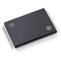
ispPAC-POWR1220AT8-02TN100I Lattice, ispPAC-POWR1220AT8-02TN100I Datasheet - Page 23

ispPAC-POWR1220AT8-02TN100I
Manufacturer Part Number
ispPAC-POWR1220AT8-02TN100I
Description
Current & Power Monitors & Regulators Prec. Power Supply Seq. Monitor Marg.
Manufacturer
Lattice
Series
ispPAC®r
Datasheet
1.ISPPAC-POWR1220AT8-02TN100I.pdf
(54 pages)
Specifications of ispPAC-POWR1220AT8-02TN100I
Mounting Style
SMD/SMT
Supply Voltage (max)
3.96 V
Supply Voltage (min)
2.8 V
Package / Case
TQFP-100
Applications
General Purpose
Voltage - Input
-0.3 V ~ 5.9 V
Voltage - Supply
2.8 V ~ 3.96 V
Current - Supply
40mA
Operating Temperature
-40°C ~ 85°C
Mounting Type
Surface Mount
Lead Free Status / RoHS Status
Lead free / RoHS Compliant
Available stocks
Company
Part Number
Manufacturer
Quantity
Price
Company:
Part Number:
ISPPAC-POWR1220AT8-02TN100I
Manufacturer:
Lattice
Quantity:
226
Company:
Part Number:
ISPPAC-POWR1220AT8-02TN100I
Manufacturer:
Lattice Semiconductor Corporation
Quantity:
10 000
Lattice Semiconductor
cuits, ADC and trim circuits. The ispPAC-POWR1220AT8 can be programmed to operate in three modes: Master
mode, Standalone mode and Slave mode. Table 1-5 summarizes the operating modes of ispPAC-POWR1220AT8.
Table 1-5. ispPAC-POWR1220AT8 Operating Modes
A divide-by-32 prescaler divides the internal 8MHz oscillator (or external clock, if selected) down to 250kHz for the
PLD clock and for the programmable timers. This PLD clock may be made available on the PLDCLK pin by closing
SW2. Each of the four timers provides independent timeout intervals ranging from 32µs to 1.96 seconds in 128
steps.
Digital Outputs
The ispPAC-POWR1220AT8 provides 20 digital outputs, HVOUT[1:4] and OUT[5:20]. Outputs OUT[5:20] are per-
manently configured as open drain to provide a high degree of flexibility when interfacing to logic signals, LEDs,
opto-couplers, and power supply control inputs. The HVOUT[1:4] pins can be configured as either high voltage FET
drivers or open drain outputs. Each of these outputs may be controlled either from the PLD or from the I
determination whether a given output is under PLD or I
13). For further details on controlling the outputs through I
data sheet.
Figure 1-13. Digital Output Pin Configuration
High-Voltage Outputs
In addition to being usable as digital open-drain outputs, the ispPAC-POWR1220AT8’s HVOUT1-HVOUT4 output
pins can be programmed to operate as high-voltage FET drivers. Figure 1-14 shows the details of the HVOUT gate
drivers. Each of these outputs may be controlled from the PLD or from the I
details on controlling the outputs through I
Operating Mode
Standalone
Master
Slave
Timer
Closed
Closed
Open
SW0
Closed
Closed
Open
SW1
When only one ispPAC-POWR1220AT8 is used.
When more than one ispPAC-POWR1220AT8 is
used in a board, one of them should be configured
to operate in this mode.
When more than one ispPAC-POWR1220AT8s is
used in a board. Other than the master, the rest of
the ispPAC-POWR1220AT8s should be pro-
grammed as slaves.
Digital Control
from I
from PLD
Digital Control
2
C, please see the I
2
C Register
2
Condition
1-23
C control may be made on a pin-by-pin basis (see Figure 1-
2
C, please see the I
2
C/SMBUS Interface section of this data sheet.
OUTx
ispPAC-POWR1220AT8 Data Sheet
Pin
2
C bus (see Figure 1-14). For further
2
C/SMBUS Interface section of this
MCLK pin tristated
MCLK pin outputs 8MHz clock
MCLK pin is input
Comments
2
C bus. The


