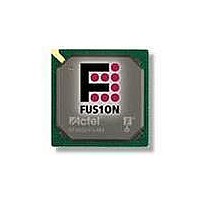
AFS600-FGG256 Actel, AFS600-FGG256 Datasheet - Page 276

AFS600-FGG256
Manufacturer Part Number
AFS600-FGG256
Description
FPGA - Field Programmable Gate Array 600K System Gates
Manufacturer
Actel
Datasheet
1.AFS600-PQG208.pdf
(330 pages)
Specifications of AFS600-FGG256
Processor Series
AFS600
Core
IP Core
Maximum Operating Frequency
1098.9 MHz
Number Of Programmable I/os
119
Data Ram Size
110592
Supply Voltage (max)
1.575 V
Maximum Operating Temperature
+ 70 C
Minimum Operating Temperature
0 C
Development Tools By Supplier
AFS-Eval-Kit, AFS-BRD600, FlashPro 3, FlashPro Lite, Silicon-Explorer II, Silicon-Sculptor 3, SI-EX-TCA
Mounting Style
SMD/SMT
Supply Voltage (min)
1.425 V
Number Of Gates
600 K
Package / Case
FPBGA-256
Lead Free Status / RoHS Status
Lead free / RoHS Compliant
Available stocks
Company
Part Number
Manufacturer
Quantity
Price
Company:
Part Number:
AFS600-FGG256
Manufacturer:
Actel
Quantity:
135
Part Number:
AFS600-FGG256
Manufacturer:
ACTEL/爱特
Quantity:
20 000
Company:
Part Number:
AFS600-FGG256I
Manufacturer:
Microsemi SoC
Quantity:
10 000
Company:
Part Number:
AFS600-FGG256K
Manufacturer:
Microsemi SoC
Quantity:
10 000
- Current page: 276 of 330
- Download datasheet (13Mb)
DC and Power Characteristics
3- 26
1. The PLL dynamic contribution depends on the input clock frequency, the number of output clock signals generated by the
PLL, and the frequency of each output clock. If a PLL is used to generate more than one output clock, include each output
clock in the formula output clock by adding its corresponding contribution (P
contribution.
RAM Dynamic Contribution—P
PLL/CCC Dynamic Contribution—P
Nonvolatile Memory Dynamic Contribution—P
Crystal Oscillator Dynamic Contribution—P
Operating Mode
P
Standby Mode and Sleep Mode
P
Operating Mode
P
Standby Mode and Sleep Mode
P
Operating Mode
P
P
Standby Mode and Sleep Mode
P
Operating Mode
P
Standby Mode
P
Sleep Mode
P
MEMORY
MEMORY
PLL
PLL
NVM
NVM
NVM
XTL-OSC
XTL-OSC
XTL-OSC
N
F
β
page
β
F
F
F
The NVM dynamic power consumption is a piecewise linear function of frequency.
N
β
F
READ-CLOCK
WRITE-CLOCK
CLKIN
CLKOUT
READ-NVM
BLOCKS
2
3
= P
NVM-BLOCKS
4
= 0 W
= N
= N
= 0 W
the RAM enable rate for write operations—guidelines are provided in
is the NVM enable rate for read operations. Default is 0 (NVM mainly in idle state).
is the RAM enable rate for read operations—guidelines are provided in
AC13
3-27.
NVM-BLOCKS
NVM-BLOCKS
= P
= P
= 0 W
= (N
= 0 W
is the input clock frequency.
is the output clock frequency.
is the number of RAM blocks used in the design.
AC18
AC18
* F
BLOCKS
is the NVM read clock frequency.
CLKOUT
is the memory read clock frequency.
is the number of NVM blocks used in the design (2 inAFS600).
is the memory write clock frequency.
*
*
* P
β
β
AC11
4
4
* P
*(P
AC15
AC16
*
β
MEMORY
2
* F
+ P
* F
READ-NVM
READ-CLOCK
PLL
AC17
R e visio n 1
1
* F
READ-NVM
when F
XTL-OSC
) + (N
NVM
READ-NVM
BLOCKS
when F
AC14
* P
READ-NVM
* F
≤ 33 MHz,
AC12
CLKOUT
*
β
> 33 MHz
3
Table 3-17 on page
product) to the total PLL
* F
WRITE-CLOCK
Table 3-17 on
)
3-27.
Related parts for AFS600-FGG256
Image
Part Number
Description
Manufacturer
Datasheet
Request
R

Part Number:
Description:
AFS600-1FGG256I
Manufacturer:
Actel
Datasheet:

Part Number:
Description:
AFS600-2FGG256I
Manufacturer:
Actel
Datasheet:


