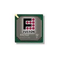
AFS600-FGG256 Actel, AFS600-FGG256 Datasheet - Page 43

AFS600-FGG256
Manufacturer Part Number
AFS600-FGG256
Description
FPGA - Field Programmable Gate Array 600K System Gates
Manufacturer
Actel
Datasheet
1.AFS600-PQG208.pdf
(330 pages)
Specifications of AFS600-FGG256
Processor Series
AFS600
Core
IP Core
Maximum Operating Frequency
1098.9 MHz
Number Of Programmable I/os
119
Data Ram Size
110592
Supply Voltage (max)
1.575 V
Maximum Operating Temperature
+ 70 C
Minimum Operating Temperature
0 C
Development Tools By Supplier
AFS-Eval-Kit, AFS-BRD600, FlashPro 3, FlashPro Lite, Silicon-Explorer II, Silicon-Sculptor 3, SI-EX-TCA
Mounting Style
SMD/SMT
Supply Voltage (min)
1.425 V
Number Of Gates
600 K
Package / Case
FPBGA-256
Lead Free Status / RoHS Status
Lead free / RoHS Compliant
Available stocks
Company
Part Number
Manufacturer
Quantity
Price
Company:
Part Number:
AFS600-FGG256
Manufacturer:
Actel
Quantity:
135
Part Number:
AFS600-FGG256
Manufacturer:
ACTEL/爱特
Quantity:
20 000
Company:
Part Number:
AFS600-FGG256I
Manufacturer:
Microsemi SoC
Quantity:
10 000
Company:
Part Number:
AFS600-FGG256K
Manufacturer:
Microsemi SoC
Quantity:
10 000
- Current page: 43 of 330
- Download datasheet (13Mb)
Global Input Selections
Each global buffer, as well as the PLL reference clock, can be driven from one of the following
22):
Notes:
1. Represents the global input pins. Globals have direct access to the clock conditioning block and are not
2. Instantiate the routed clock source input as follows:
3. LVDS-based clock sources are available in the east and west banks on all Fusion devices.
Figure 2-22 • Clock Input Sources Including CLKBUF, CLKBUF_LVDS/LVPECL, and CLKINT
Each shaded box represents an
input buffer called out by the
appropriate name: INBUF or
INBUF_LVDS/LVPECL.
•
•
•
routed via the FPGA fabric. Refer to the
information.
a) Connect the output of a logic element to the clock input of the PLL, CLKDLY, or CLKINT macro.
b) Do not place a clock source I/O (INBUF or INBUF_LVPECL/LVDS) in a relevant global pin location.
Sample Pin Names
3 dedicated single-ended I/Os using a hardwired connection
2 dedicated differential I/Os using a hardwired connection
The FPGA core
GAA[0:2]: GA represents global in the northwest corner
of the device. A[0:2]: designates specific A clock source.
GAA0
GAA1
GAA2
1
1
1
+
+
"User I/O Naming Convention" section on page 2-160
R e v i s i o n 1
To Core
Actel Fusion Family of Mixed Signal FPGAs
(from FPGA core)
Routed Clock
Source for CCC
(CLKA or CLKB or CLKC)
2
(Figure 2-
for more
2- 27
Related parts for AFS600-FGG256
Image
Part Number
Description
Manufacturer
Datasheet
Request
R

Part Number:
Description:
AFS600-1FGG256I
Manufacturer:
Actel
Datasheet:

Part Number:
Description:
AFS600-2FGG256I
Manufacturer:
Actel
Datasheet:


