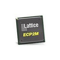
LFE2M20SE-5FN256C Lattice, LFE2M20SE-5FN256C Datasheet - Page 35

LFE2M20SE-5FN256C
Manufacturer Part Number
LFE2M20SE-5FN256C
Description
FPGA - Field Programmable Gate Array 19K LUTs 140 I/O S-Ser SERDES DSP -5
Manufacturer
Lattice
Datasheet
1.LFE2-12SE-6FN256C.pdf
(389 pages)
Specifications of LFE2M20SE-5FN256C
Number Of Macrocells
19000
Maximum Operating Frequency
311 MHz
Number Of Programmable I/os
140
Data Ram Size
1246208
Supply Voltage (max)
1.26 V
Maximum Operating Temperature
+ 85 C
Minimum Operating Temperature
0 C
Mounting Style
SMD/SMT
Supply Voltage (min)
1.14 V
Package / Case
FPBGA-256
Lead Free Status / RoHS Status
Lead free / RoHS Compliant
Available stocks
Company
Part Number
Manufacturer
Quantity
Price
Company:
Part Number:
LFE2M20SE-5FN256C
Manufacturer:
Lattice Semiconductor Corporation
Quantity:
10 000
- Current page: 35 of 389
- Download datasheet (5Mb)
Lattice Semiconductor
By combining input blocks of the complementary PIOs and sharing some registers from output blocks, a gearbox
function can be implemented, which takes a double data rate signal applied to PIOA and converts it as four data
streams, IPOS0A, IPOS1A, IPOS0B and IPOS1B. Figure 2-29 shows the diagram using this gearbox function. For
more information about this topic, please see information regarding additional documentation at the end of this
data sheet.
The signal DDRCLKPOL controls the polarity of the clock used in the synchronization registers. It ensures ade-
quate timing when data is transferred from the DQS to the system clock domain. For further information about this
topic, see the DDR Memory section of this data sheet.
Figure 2-29. Input Register Block for Left, Right and Bottom Edges
CLK0 (of PIO B)
CLK0 (of PIO A)
DDRCLKPOL
DDRCLKPOL
(From sysIO
(From sysIO
Routing
Routing
DEL [3:0]
From
From
Buffer)
Buffer)
DEL [3:0]
Delayed
Delayed
DI
DI
DQS
DQS
CLKA
CLKB
*Shared with output register
**Selected PIO.
True PIO (A) in LVDS I/O Pair
Comp PIO (B) in LVDS I/O Pair
Dynamic Delay
Dynamic Delay
Fixed Delay
Fixed Delay
0
1
0
1
0
1
0
1
DDR Registers
DDR Registers
D
D
D
D
D-Type
D-Type
D-Type
D-Type
Q
Q
Q
Q
D1
D1
0
1
D
D
D-Type
DDRSRC
D-Type
D0
0
1
Q
Q
2-32
Gearbox Configuration Bit
D2
D0
D2
0
1
0
1
SDR & Sync
SDR & Sync
Registers
Registers
D
D
D
D
/LATCH
/LATCH
/LATCH
/LATCH
D-Type
D-Type
D-Type
D-Type
LatticeECP2/M Family Data Sheet
Q
Q
Q
Q
Note: Simplified version does not
show CE and SET/RESET details
Clock Transfer Registers
Clock Transfer Registers
D
D
D
D
D-Type*
D-Type*
D-Type*
D-Type*
Q
Q
Q
Q
INCK**
To DQS Delay Block**
INDD
IPOS0A
QPOS0A
IPOS1A
QPOS1A
INCK**
To DQS Delay Block**
INDD
IPOS0B
QPOS0B
IPOS1B
QPOS1B
Architecture
Routing
Routing
To
To
Related parts for LFE2M20SE-5FN256C
Image
Part Number
Description
Manufacturer
Datasheet
Request
R

Part Number:
Description:
FPGA - Field Programmable Gate Array 19K LUTs 304 I/O S-Ser SERDES DSP -5
Manufacturer:
Lattice
Datasheet:
Part Number:
Description:
FPGA LatticeECP2M Family 19000 Cells 90nm (CMOS) Technology 1.2V 484-Pin FBGA
Manufacturer:
LATTICE SEMICONDUCTOR
Datasheet:

Part Number:
Description:
FPGA LatticeECP2M Family 19000 Cells 90nm (CMOS) Technology 1.2V 256-Pin FBGA
Manufacturer:
Lattice
Datasheet:

Part Number:
Description:
IC FPGA 20KLUTS 140I/O 256-BGA
Manufacturer:
Lattice
Datasheet:

Part Number:
Description:
IC FPGA 20KLUTS 140I/O 256-BGA
Manufacturer:
Lattice
Datasheet:

Part Number:
Description:
IC FPGA 20KLUTS 304I/O 484-BGA
Manufacturer:
Lattice
Datasheet:

Part Number:
Description:
IC FPGA 19KLUTS 484FGPBGA
Manufacturer:
Lattice
Datasheet:

Part Number:
Description:
FPGA - Field Programmable Gate Array 19K LUTs 304 I/O S-Ser SERD DSP -6
Manufacturer:
Lattice

Part Number:
Description:
FPGA - Field Programmable Gate Array 19K LUTs 304 I/O S-Ser SERD DSP -7
Manufacturer:
Lattice

Part Number:
Description:
FPGA - Field Programmable Gate Array 19K LUTs 140 I/O S-Ser SERD DSP -6 I
Manufacturer:
Lattice

Part Number:
Description:
FPGA - Field Programmable Gate Array 19K LUTs 140 I/O S-Ser SERD DSP -6
Manufacturer:
Lattice

Part Number:
Description:
FPGA - Field Programmable Gate Array 19K LUTs 304 I/O S-Ser SERDES DSP -5
Manufacturer:
Lattice

Part Number:
Description:
FPGA - Field Programmable Gate Array 19K LUTs 304 I/O S-Ser SERD DSP -6 I
Manufacturer:
Lattice


