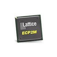
LFE2M20SE-5FN256C Lattice, LFE2M20SE-5FN256C Datasheet - Page 99

LFE2M20SE-5FN256C
Manufacturer Part Number
LFE2M20SE-5FN256C
Description
FPGA - Field Programmable Gate Array 19K LUTs 140 I/O S-Ser SERDES DSP -5
Manufacturer
Lattice
Datasheet
1.LFE2-12SE-6FN256C.pdf
(389 pages)
Specifications of LFE2M20SE-5FN256C
Number Of Macrocells
19000
Maximum Operating Frequency
311 MHz
Number Of Programmable I/os
140
Data Ram Size
1246208
Supply Voltage (max)
1.26 V
Maximum Operating Temperature
+ 85 C
Minimum Operating Temperature
0 C
Mounting Style
SMD/SMT
Supply Voltage (min)
1.14 V
Package / Case
FPBGA-256
Lead Free Status / RoHS Status
Lead free / RoHS Compliant
Available stocks
Company
Part Number
Manufacturer
Quantity
Price
Company:
Part Number:
LFE2M20SE-5FN256C
Manufacturer:
Lattice Semiconductor Corporation
Quantity:
10 000
- Current page: 99 of 389
- Download datasheet (5Mb)
LatticeECP2/M sysCONFIG Port Timing Specifications (Continued)
Lattice Semiconductor
Figure 3-14. sysCONFIG Parallel Port Read Cycle
t
t
1. Re-toggling the PROGRAMN pin is not permitted until the INITN pin is high. Avoid consecutive toggling of the PROGRAMN.
2. For SED (Soft Error Detect), the SEDCLKIN operating frequency must be at least 20MHz. SEDCLKIN is derived from Master Clock Fre-
Master Clock Frequency
Duty Cycle
SUSPI
HSPI
quency that has a +/-30% variation..
Parameter
Parameter
WRITEN
SOSPI Data Setup Time Before CCLK
SOSPI Data Hold Time After CCLK
CCLK
CS1N
BUSY
D[0:7]
*n = last byte of read cycle.
CSN
Selected value - 30%
Over Recommended Operating Conditions
Min.
40
t
t
Description
SUCS
SUWD
Byte 0
t
BSCL
3-47
Byte 1
t
CORD
Selected value + 30%
Max.
t
60
DCB
DC and Switching Characteristics
LatticeECP2/M Family Data Sheet
t
Byte 2
BSCYC
t
BSCH
Byte n*
Min.
t
t
7
2
HCS
HWD
Units
MHz
Max.
%
—
—
Units
ns
ns
Related parts for LFE2M20SE-5FN256C
Image
Part Number
Description
Manufacturer
Datasheet
Request
R

Part Number:
Description:
FPGA - Field Programmable Gate Array 19K LUTs 304 I/O S-Ser SERDES DSP -5
Manufacturer:
Lattice
Datasheet:
Part Number:
Description:
FPGA LatticeECP2M Family 19000 Cells 90nm (CMOS) Technology 1.2V 484-Pin FBGA
Manufacturer:
LATTICE SEMICONDUCTOR
Datasheet:

Part Number:
Description:
FPGA LatticeECP2M Family 19000 Cells 90nm (CMOS) Technology 1.2V 256-Pin FBGA
Manufacturer:
Lattice
Datasheet:

Part Number:
Description:
IC FPGA 20KLUTS 140I/O 256-BGA
Manufacturer:
Lattice
Datasheet:

Part Number:
Description:
IC FPGA 20KLUTS 140I/O 256-BGA
Manufacturer:
Lattice
Datasheet:

Part Number:
Description:
IC FPGA 20KLUTS 304I/O 484-BGA
Manufacturer:
Lattice
Datasheet:

Part Number:
Description:
IC FPGA 19KLUTS 484FGPBGA
Manufacturer:
Lattice
Datasheet:

Part Number:
Description:
FPGA - Field Programmable Gate Array 19K LUTs 304 I/O S-Ser SERD DSP -6
Manufacturer:
Lattice

Part Number:
Description:
FPGA - Field Programmable Gate Array 19K LUTs 304 I/O S-Ser SERD DSP -7
Manufacturer:
Lattice

Part Number:
Description:
FPGA - Field Programmable Gate Array 19K LUTs 140 I/O S-Ser SERD DSP -6 I
Manufacturer:
Lattice

Part Number:
Description:
FPGA - Field Programmable Gate Array 19K LUTs 140 I/O S-Ser SERD DSP -6
Manufacturer:
Lattice

Part Number:
Description:
FPGA - Field Programmable Gate Array 19K LUTs 304 I/O S-Ser SERDES DSP -5
Manufacturer:
Lattice

Part Number:
Description:
FPGA - Field Programmable Gate Array 19K LUTs 304 I/O S-Ser SERD DSP -6 I
Manufacturer:
Lattice


