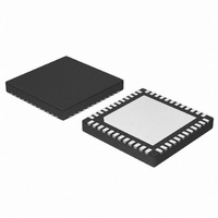
NCP5393MNR2G ON Semiconductor, NCP5393MNR2G Datasheet

NCP5393MNR2G
Specifications of NCP5393MNR2G
Available stocks
Related parts for NCP5393MNR2G
NCP5393MNR2G Summary of contents
Page 1
... ON Semiconductor Soldering and Mounting Techniques Reference Manual, SOLDERRM/D. © Semiconductor Components Industries, LLC, 2008 March, 2008 - Rev. 1 phases and one V DD DDNB and DD regulators. Dynamic DDNB NCP5393MNR2G †For information on tape and reel specifications, and V Outputs DD DDNB and V Outputs DD DDNB and ...
Page 2
NCP5393 48 1 VCCA GND COMP FB DROOP VS+ VS- OFFSET DIFFOUT VFIX 12VMON PSI_L Figure 1. Pinout http://onsemi.com 2 VID1 VID0 NB_COMP NB_FB NB_DROOP NB_VS+ NB_VS- NB_OFFSET NB_DIFFOUT ROSC VID5 VID4 ...
Page 3
NB_VS NB_VS- NB_DIFFOUT Diff Amp + NB_FB 1 Error Amp NB_COMP NB_DROOP Gain = 1 Droop Amplifier 1 NB_CS + - NB_CSN NORMAL OPERATION Gain = 6 BOOT_VID & VFIX MODES NB NB_SRL OUT ...
Page 4
NCP5393 Figure 3. NCP5393 Configured for Phases, with Optional Droop http://onsemi.com 4 ...
Page 5
NCP5393 PIN DESCRIPTIONS Pin No. Symbol 1 VCCA 5 V supply pin for the NCP5393. The V pin and GND (preferably returned to the package flag). 2 GND Small-signal power supply return. This pin should be tied directly to the ...
Page 6
NCP5393 PIN DESCRIPTIONS Pin No. Symbol 32 NB_DROOP Voltage output signal proportional to total current drawn from the VDDNB regulator. Used when load line operation (“droop”) is desired. 33 NB_FB Voltage error amplifier inverting input for the V 34 NB_COMP ...
Page 7
ABSOLUTE MAXIMUM RATINGS ELECTRICAL INFORMATION Pin Symbol 12VMON VCC COMP, NB_COMP DROOP, NB_DROOP DIFFOUT, NB_DIFFOUT DRVON, NB_DRVON PWRGOOD VS+, NB_VS+ VS-, NB_VS- ROSC All Other Pins Stresses exceeding Maximum Ratings may damage the device. Maximum Ratings are stress ratings only. ...
Page 8
ELECTRICAL CHARACTERISTICS (Unless otherwise stated: 0°CvT Parameter ERROR AMPLIFIERS (V & DDNB Input Bias Current Input Offset Voltage (Note 1.3V Open Loop DC Gain C Open Loop Unity Gain Bandwidth C Open ...
Page 9
ELECTRICAL CHARACTERISTICS (Unless otherwise stated: 0°CvT Parameter CURRENT SENSE AMPLIFIERS (V & Input Bias Current CSx = CSxN = 1.4 V Common Mode Input Voltage Range Differential Mode Input Voltage Range (Note 3) Input Offset Voltage (Note 3) ...
Page 10
ELECTRICAL CHARACTERISTICS (Unless otherwise stated: 0°CvT Parameter PWRGOOD OUTPUT PWRGOOD Upper Threshold V PWRGOOD Lower Threshold V PWM OUTPUTS (V & DDNB Sourcing 500 mA Output Voltage (High) Output Voltage (Mid) R Sinking 500 mA Output Voltage ...
Page 11
ELECTRICAL CHARACTERISTICS (Unless otherwise stated: 0°CvT Parameter CURRENT LIMIT Current Sense Amp to ILIM Gain 20 mV < (CSx - CSxN) < (CS inputs tied) ILIM Pin Input Bias Current ILIM Pin Working Voltage Range (Note 3) ILIM ...
Page 12
T , JUNCTION TEMPERATURE (°C) J Figure 3. I Current vs. Temperature CC 4.5 V Increasing Voltage CCP 4.0 V Decreasing Voltage CCP 3.5 3 JUNCTION ...
Page 13
Functional Description General NCP5393 is a universal CPU hybrid power Controller compatible with both Parallel VID interface (PVI) and Serial VID interface (SVI) protocols for AMD Processors. The Controller implements a single-phase control architecture to provide the Northbridge (NB) voltage ...
Page 14
VDDNB oscillator will free-run at a frequency which is nominally 1.25 ratio of f CPU Support NCP5393 is able to detect the CPU it is going to supply and configure itself to PVI or SVI mode. When in ...
Page 15
Table 2. SIX-BIT PARALLEL VID CODES in PVI Modes SVID[5:0] V (V) SVID[5:0] OUT 00_0000 1.5500 00_0001 1.5250 00_0010 1.5000 00_0011 1.4750 00_0100 1.4500 00_0101 1.4250 00_0110 1.4000 10_0111 1.3750 00_1000 1.3500 00_1001 1.3250 00_1010 1.3000 00_1011 1.2750 00_1100 1.2500 ...
Page 16
Table 3. SEVEN-BIT SERIAL VID CODES for SVI Mode SVID[6:0] V (V) SVID[6:0] OUT 000_0000 1.5500 010_0000 000_0001 1.5375 010_0001 000_0010 1.5250 010_0010 000_0011 1.5125 010_0011 000_0100 1.5000 010_0100 000_0101 1.4875 010_0101 000_0110 1.4750 010_0110 000_0111 1.4625 010_0111 000_1000 1.4500 ...
Page 17
Turn-On VDDIO Command ENABLE PVIEN/ VID[1] VID[1] Low at Rise of Enable Selects SVI Operation BOOT VID MSB SVC/ VID[3] SVD/ VID[2] BOOT VID LSB VDD and VDDNB Soft-Start is PWRGOOD Complete CPU Can Begin PWROK Serial ...
Page 18
Protection Features: The NCP5393 handles many protection features. Undervoltage lockout, Over Overvoltage, Under voltage, Soft-Start etc are the main features. All the fault responses of the NCP5393 are listed in Table 5. Undervoltage Lockout An undervoltage lockout (UVLO) senses the ...
Page 19
Table 5. Fault Responses PWM OUTPUT(s) CONDITION PWRGOOD VDD Global All to High-Z Latched Low OCP NB OCP All to High-Z Latched Low VDD Affected Unaffected Per-Phase phase set to Current Limit Low or Mid state Output OVP Held Low ...
Page 20
Programming the Current Limit and the Oscillator Frequency The demo board is set for an operating frequency of approximately 330 kHz. The ROSC pin provides a 2.0 V reference voltage which is divided down with a resistor divider and fed ...
Page 21
OUTPUT OFFSET VOLTAGES External offset voltages from 800 mV `above the DAC' can be added for the V Offset is set by a resistor divider from V factors change by the same amount: For example: For 0 ...
Page 22
In some modes, significant offset above VDAC could cause unpredictable results harmful. The NCP5393 avoids such modes. MODE VDD OFFSET PVI (Soft-Start) NO PVI (Normal Operation) YES SVI (Soft-Start) NO SVI (Boot VID) NO SVI (Normal Operation) YES ...
Page 23
... 48X *For additional information on our Pb-Free strategy and soldering 0. details, please download the ON Semiconductor Soldering and Mounting Techniques Reference Manual, SOLDERRM/D. 0.05 C NOTE 3 N. American Technical Support: 800-282-9855 Toll Free USA/Canada Europe, Middle East and Africa Technical Support: Phone: 421 33 790 2910 Japan Customer Focus Center ...


