LM2842XMK-ADJEV/NOPB National Semiconductor, LM2842XMK-ADJEV/NOPB Datasheet - Page 9
LM2842XMK-ADJEV/NOPB
Manufacturer Part Number
LM2842XMK-ADJEV/NOPB
Description
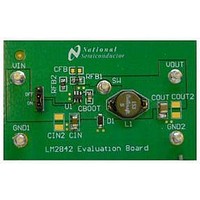
EVAL BOARD FOR LM2842XMK-ADJ
Manufacturer
National Semiconductor
Specifications of LM2842XMK-ADJEV/NOPB
Silicon Manufacturer
National
Silicon Core Number
LM2842
Kit Application Type
Power Management - Voltage Regulator
Application Sub Type
Buck Regulator
Kit Contents
Board
Lead Free Status / RoHS Status
Lead free / RoHS Compliant


rent rating for the diode should be equal to the maximum
output current for best reliability in most applications. In cases
where the input voltage is much greater than the output volt-
age the average diode current is lower. In this case it is
possible to use a diode with a lower average current rating,
approximately (1-D)I
should be higher than the maximum load current. A 0.5A to
1A rated diode is a good starting point.
LAYOUT CONSIDERATIONS
To reduce problems with conducted noise pick up, the ground
side of the feedback network should be connected directly to
the GND pin with its own connection. The feedback network,
resistors R1 and R2, should be kept close to the FB pin, and
away from the inductor to minimize coupling noise into the
OUT
, however the peak current rating
9
feedback pin. The input bypass capacitor C
close to the V
which effects input voltage ripple of the IC. The inductor L1
should be placed close to the SW pin to reduce magnetic and
electrostatic noise. The output capacitor, C
placed close to the junction of L1 and the diode D1. The L1,
D1, and C
conducted and radiated noise and increase overall efficiency.
The ground connection for the diode, C
be as small as possible and tied to the system ground plane
in only one spot (preferably at the C
imize conducted noise in the system ground plane. For more
detail on switching power supply layout considerations see
Application Note AN-1149: Layout Guidelines for Switching
Power Supplies.
OUT
IN
trace should be as short as possible to reduce
pin. This will reduce copper trace resistance
OUT
ground point) to min-
IN
, and C
IN
must be placed
OUT
www.national.com
OUT
should be
should
Related parts for LM2842XMK-ADJEV/NOPB
Image
Part Number
Description
Manufacturer
Datasheet
Request
R

Part Number:
Description:
IC REG ADJ 600MA BUCK TSOT23-6
Manufacturer:
National Semiconductor
Datasheet:

Part Number:
Description:
Manufacturer:
National Semiconductor
Datasheet:
Part Number:
Description:
National Semiconductor [8-Bit D/A Converter]
Manufacturer:
National Semiconductor
Datasheet:
Part Number:
Description:
National Semiconductor [Media Coprocessor]
Manufacturer:
National Semiconductor
Datasheet:
Part Number:
Description:
Digitally Controlled Tone and Volume Circuit with Stereo Audio Power Amplifier, Microphone Preamp Stage and National 3D Sound
Manufacturer:
National Semiconductor
Datasheet:
Part Number:
Description:
Digitally Controlled Tone and Volume Circuit with Stereo Audio Power Amplifier, Microphone Preamp Stage and National 3D Sound
Manufacturer:
National Semiconductor
Datasheet:
Part Number:
Description:
AC97 Rev 2 Codec with Sample Rate Conversion and National 3D Sound
Manufacturer:
National Semiconductor
Part Number:
Description:
Manufacturer:
National Semiconductor
Datasheet:
Part Number:
Description:
Manufacturer:
National Semiconductor
Datasheet:
Part Number:
Description:
General Purpose, Low Voltage, Low Power, Rail-to-Rail Output Operational Amplifiers
Manufacturer:
National Semiconductor
Datasheet:
Part Number:
Description:
8-bit 20 MSPS flash A/D converter.
Manufacturer:
National Semiconductor
Datasheet:
Part Number:
Description:
Low Noise Quad Operational Amplifier
Manufacturer:
National Semiconductor
Datasheet:
Part Number:
Description:
Quad Differential Line Receivers
Manufacturer:
National Semiconductor
Datasheet:
Part Number:
Description:
Quad High Speed Trapezoidal? Bus Transceiver
Manufacturer:
National Semiconductor
Datasheet: