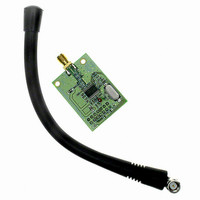
EVAL-ADF7012DBZ3 Analog Devices Inc, EVAL-ADF7012DBZ3 Datasheet - Page 13

EVAL-ADF7012DBZ3
Manufacturer Part Number
EVAL-ADF7012DBZ3
Description
BOARD EVALUATION DB3 FOR ADF7012
Manufacturer
Analog Devices Inc
Type
Transmitterr
Specifications of EVAL-ADF7012DBZ3
Frequency
1GHz
For Use With/related Products
ADF7012
Lead Free Status / RoHS Status
Lead free / RoHS Compliant
The output buffer to CLK
the function register high. On power-up, this bit is set high.
The output buffer can drive up to a 20 pF load with a 10% rise
time at 4.8 MHz. Faster edges can result in some spurious
feedthrough to the output. A small series resistor (50 Ω) can
be used to slow the clock edges to reduce these spurs at F
LOOP FILTER
The loop filter integrates the current pulses from the charge
pump to form a voltage that tunes the output of the VCO to the
desired frequency. It also attenuates spurious levels generated by
the PLL. A typical loop filter design is shown in Figure 29.
In FSK, it is recommended that the loop bandwidth be a
minimum of two to three times the data rate. Widening the
LBW excessively reduces the time spent jumping between
frequencies, but results in reduced spurious attenuation. See
the Tips on Designing the Loop Filter section.
For OOK/ASK systems, a wider loop bandwidth than for FSK
systems is desirable. The sudden large transition between two
power levels results in VCO pulling (VCO temporarily goes to
incorrect frequency) and can cause a wider output spectrum.
By widening the loop bandwidth a minimum of 10× the data
rate, VCO pulling is minimized because the loop settles quickly
back to the correct frequency. A free design tool, the ADI SRD
Design Studio™, can be used to design loop filters for the Analog
Devices family of transmitters.
VOLTAGE-CONTROLLED OSCILLATOR (VCO)
The ADF7012 features an on-chip VCO with an external tank
inductor, which is used to set the frequency range. The center
frequency of oscillation is governed by the internal varactor
capacitance and that of the external inductor combined with
the bond-wire inductance. An approximation for this is given
in Equation 4. For a more accurate selection of the inductor,
see the section Choosing the External Inductor Value.
F
VCO
OSC1
=
PUMP OUT
π 2
CHARGE
DIVIDER
1 TO 15
(
L
INT
Figure 29. Typical Loop Filter
Figure 28. CLKOUT Stage
+
L
EXT
OUT
)
1
is enabled by setting Bit DB4 in
×
÷2
(
C
DV
VAR
DD
+
C
FIXED
VCO
CLK
CLK
ENABLE BIT
)
OUT
OUT
CLK
(4)
.
Rev. A | Page 13 of 28
The varactor capacitance can be adjusted in software to increase
the effective VCO range by writing to the VA1 and VA2 bits in
the R register. Under typical conditions, setting VA1 and VA2
high increases the center frequency by reducing the varactor
capacitance by approximately 1.3 pF.
Figure 37 shows the variation of VCO gain with frequency.
VCO gain is important in determining the loop filter design—
predictable changes in VCO gain resulting in a change in the
loop filter bandwidth can be offset by changing the charge-
pump current in software.
VCO Bias Current
VCO bias current may be adjusted using bits VB1 to VB4 in the
function register. Additional bias current will reduce spurious
levels, but increase overall current consumption in the part. A
bias value of 0x5 should ensure oscillation at most frequencies
and supplies. Settings 0x0, 0xE , and 0xF are not recommended.
Setting 0x3 and Setting 0x4 are recommended under most
conditions. Improved phase noise can be achieved for lower
bias currents.
VOLTAGE REGULATORS
There are two band gap voltage regulators on the ADF7012
providing a stable 2.25 V internal supply: a 2.2 μF capacitor
(X5R, NP0) to ground at C
should be used to ensure stability. The internal reference
ensures consistent performance over all supplies and reduces
the current consumption of each of the blocks.
The combination of regulators, band gap reference, and biasing
typically consume 1.045 mA at 3.0 V and can be powered down
by bringing the CE line low. The serial interface is supplied by
Regulator 1, so powering down the CE line causes the contents
of the registers to be lost. The CE line must be high and the reg-
ulators must be fully powered on to write to the serial interface.
Regulator power-on time is typically 100 μs and should be taken
into account when writing to the ADF7012 after power-up.
Alternatively, regulator status may be monitored at the MUXOUT
pin once CE has been asserted, because MUXOUT defaults to
the regulator ready signal. Once Regulator_ready is high, the
regulator is powered up and the serial interface is active.
FSK MODULATION
FSK modulation is performed internally in the PLL loop by
switching the value of the N register based on the status of
the TxDATA line. The TxDATA line is sampled at each cycle
of the PFD block (every 1/F
makes a low-to-high transition, an N value representing the
deviation frequency is added to the N value representing the
center frequency. Immediately the loop begins to lock to the
new frequency of F
makes a high-to-low transition, the N value representing the
deviation is subtracted from the PLL N value representing the
center frequency and the loop transitions to F
CENTER
+ F
REG1
DEVIATION
PFD
and a 470 nF capacitor at C
seconds). When TxDATA
. Conversely, when TxDATA
CENTER
ADF7012
− F
DEVIATION
REG2
.


