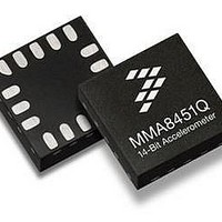
MMA8452QT Freescale Semiconductor, MMA8452QT Datasheet - Page 44

MMA8452QT
Manufacturer Part Number
MMA8452QT
Description
IC ACCELEROMETER 3AXIS 16QFN
Manufacturer
Freescale Semiconductor
Series
MMAr
Datasheet
1.MMA8452QT.pdf
(50 pages)
Specifications of MMA8452QT
Axis
X, Y, Z
Acceleration Range
± 2g, 4g, 8g
Sensitivity
1024 count/g, 2048 count/g, 4096 count/g
Voltage - Supply
1.95 V ~ 3.6 V
Output Type
Digital
Bandwidth
800Hz
Interface
I²C
Mounting Type
Surface Mount
Package / Case
16-VFQFN
Sensing Axis
X, Y, Z
Acceleration
2 g, 4 g, 8 g
Digital Output - Number Of Bits
8 bit, 12 bit
Supply Voltage (max)
3.6 V
Supply Voltage (min)
1.95 V
Maximum Operating Temperature
+ 85 C
Minimum Operating Temperature
- 40 C
Digital Output - Bus Interface
I2C
Shutdown
Yes
Lead Free Status / RoHS Status
Lead free / RoHS Compliant
Available stocks
Company
Part Number
Manufacturer
Quantity
Price
Part Number:
MMA8452QT
Manufacturer:
FREESCALE
Quantity:
20 000
0x2E CTRL_REG5 Register (Read/Write)
the routing table for the INT1 and INT2 interrupt pins. If the bit value is logic ‘0’ the functional block’s interrupt is routed to INT2,
and if the bit value is logic ‘1’ then the interrupt is routed to INT1. One or more functions can assert an interrupt pin; therefore a
host application responding to an interrupt should read the INT_SOURCE (0x0C) register to determine the appropriate sources
of the interrupt.
6.8
complement offset correction registers values are used to realign the Zero-g position of the X, Y , and Z-axis after device board
mount. The resolution of the offset registers is 2 mg per LSB. The 2’s complement 8-bit value would result in an offset
compensation range ±256 mg.
0x2F: OFF_X Offset Correction X Register
Table 63. OFF_X Description
0x30: OFF_Y Offset Correction Y Register
Table 64. OFF_Y Description
0x31: OFF_Z Offset Correction Z Register
Table 65. OFF_Z Description
0x2E: CTRL_REG5 Interrupt Configuration Register
0x30 OFF_Y Register (Read/Write)
0x2F OFF_X Register (Read/Write)
0x31 OFF_Z Register (Read/Write)
44
Table 62. Interrupt Configuration Register Description
MMA8452Q
INT_CFG_ASLP
The system’s interrupt controller shown in
For more information on how to calibrate the 0g Offset refer to AN4069 Offset Calibration Using the MMA8452Q. The 2’s
Bit 7
Bit 7
Interrupt Configuration
Bit 7
Bit 7
D7
D7
D7
INT_CFG_LNDPRT
INT_CFG_TRANS
INT_CFG_PULSE
INT_CFG_FF_MT
INT_CFG_DRDY
INT_CFG_ASLP
User Offset Correction Registers
D[7:0]
D[7:0]
D[7:0]
Bit 6
Bit 6
Bit 6
Bit 6
D6
D6
D6
0
X-axis offset value. Default value: 0000_0000.
Y-axis offset value. Default value: 0000_0000.
Z-axis offset value. Default value: 0000_0000.
INT_CFG_TRANS INT_CFG_LNDPRT INT_CFG_PULSE INT_CFG_FF_MT
INT1/INT2 Configuration. Default value: 0.
0: Interrupt is routed to INT2 pin; 1: Interrupt is routed to INT1 pin
INT1/INT2 Configuration. Default value: 0.
0: Interrupt is routed to INT2 pin; 1: Interrupt is routed to INT1 pin
INT1/INT2 Configuration. Default value: 0.
0: Interrupt is routed to INT2 pin; 1: Interrupt is routed to INT1 pin
INT1/INT2 Configuration. Default value: 0.
0: Interrupt is routed to INT2 pin; 1: Interrupt is routed to INT1 pin
INT1/INT2 Configuration. Default value: 0.
0: Interrupt is routed to INT2 pin; 1: Interrupt is routed to INT1 pin
INT1/INT2 Configuration. Default value: 0.
0: Interrupt is routed to INT2 pin; 1: Interrupt is routed to INT1 pin
Bit 5
Bit 5
Bit 5
Bit 5
D5
D5
D5
Figure 11
Bit 4
Bit 4
Bit 4
Bit 4
uses the corresponding bit field in the CTRL_REG5 register to determine
D4
D4
D4
Bit 3
Bit 3
Bit 3
Bit 3
D3
D3
D3
Description
Bit 2
Bit 2
Bit 2
Bit 2
D2
D2
D2
Bit 1
Bit 1
Bit 1
Bit 1
Freescale Semiconductor
D1
D1
D1
0
INT_CFG_DRDY
Bit 0
Bit 0
Bit 0
Bit 0
D0
D0
D0
Sensors


