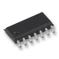
LMC660CM National Semiconductor, LMC660CM Datasheet - Page 7

LMC660CM
Manufacturer Part Number
LMC660CM
Description
OP AMP, QUAD CMOS, SMD, SOIC14, 660
Manufacturer
National Semiconductor
Datasheet
1.LMC660CM.pdf
(14 pages)
Specifications of LMC660CM
Op Amp Type
Low Input Bias
No. Of Amplifiers
4
Bandwidth
0.5MHz
Slew Rate
1.1V/µs
Supply Voltage Range
4.75V To 15.5V
Amplifier Case Style
SOIC
No. Of Pins
14
Operating Temperature
RoHS Compliant
Available stocks
Company
Part Number
Manufacturer
Quantity
Price
Part Number:
LMC660CM
Manufacturer:
NS/国半
Quantity:
20 000
Company:
Part Number:
LMC660CM/NOPB
Manufacturer:
TI
Quantity:
9 289
Company:
Part Number:
LMC660CMD-734
Manufacturer:
NS
Quantity:
351
Part Number:
LMC660CMX
Manufacturer:
TI/德州仪器
Quantity:
20 000
Company:
Part Number:
LMC660CMX/NOPB
Manufacturer:
TI
Quantity:
14 390
Part Number:
LMC660CMX/NOPB
Manufacturer:
TI/德州仪器
Quantity:
20 000
Application Hints
COMPENSATING INPUT CAPACITANCE
The high input resistance of the LMC660 op amps allows the
use of large feedback and source resistor values without
losing gain accuracy due to loading. However, the circuit will
be especially sensitive to its layout when these large-value
resistors are used.
Every amplifier has some capacitance between each input
and AC ground, and also some differential capacitance be-
tween the inputs. When the feedback network around an
amplifier is resistive, this input capacitance (along with any
additional capacitance due to circuit board traces, the
socket, etc.) and the feedback resistors create a pole in the
feedback path. In the following General Operational Amplifier
circuit, Figure 2 the frequency of this pole is
where C
including amplifier input capcitance and any stray capaci-
tance from the IC socket (if one is used), circuit board traces,
etc., and R
formula, as well as all formulae derived below, apply to
inverting and non-inverting op-amp configurations.
When the feedback resistors are smaller than a few kΩ, the
frequency of the feedback pole will be quite high, since C
generally less than 10 pF. If the frequency of the feedback
pole is much higher than the “ideal” closed-loop bandwidth
(the nominal closed-loop bandwidth in the absence of C
the pole will have a negligible effect on stability, as it will add
only a small amount of phase shift.
However, if the feedback pole is less than approximately 6 to
10 times the “ideal” −3 dB frequency, a feedback capacitor,
C
ing input of the op amp. This condition can also be stated in
terms of the amplifier’s low-frequency noise gain: To main-
tain stability a feedback capacitor will probably be needed if
where
is the amplifier’s low-frequency noise gain and GBW is the
amplifier’s gain bandwidth product. An amplifier’s low-
frequency noise gain is represented by the formula
regardless of whether the amplifier is being used in inverting
or non-inverting mode. Note that a feedback capacitor is
more likely to be needed when the noise gain is low and/or
the feedback resistor is large.
If the above condition is met (indicating a feedback capacitor
will probably be needed), and the noise gain is large enough
that:
F
, should be connected between the output and the invert-
S
P
is the total capacitance at the inverting input,
is the parallel combination of R
(Continued)
F
and R
IN
. This
S
S
is
),
7
the following value of feedback capacitor is recommended:
If
the feedback capacitor should be:
Note that these capacitor values are usually significant
smaller than those given by the older, more conservative
formula:
C
from the circuit board and socket. C
C
Using the smaller capacitors will give much higher band-
width with little degradation of transient response. It may be
necessary in any of the above cases to use a somewhat
larger feedback capacitor to allow for unexpected stray ca-
pacitance, or to tolerate additional phase shifts in the loop, or
excessive capacitive load, or to decrease the noise or band-
width, or simply because the particular circuit implementa-
tion needs more feedback capacitance to be sufficiently
stable. For example, a printed circuit board’s stray capaci-
tance may be larger or smaller than the breadboard’s, so the
actual optimum value for C
estimated using the breadboard. In most cases, the values
of C
the computed value.
S
S
consists of the amplifier’s input capacitance plus any stray capacitance
and the feedback resistors.
FIGURE 2. General Operational Amplifier Circuit
F
should be checked on the actual circuit, starting with
F
F
may be different from the one
compensates for the pole caused by
00876706
www.national.com


