LM675T National Semiconductor, LM675T Datasheet - Page 6
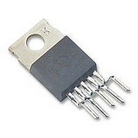
LM675T
Manufacturer Part Number
LM675T
Description
IC, OP-AMP, 5.5MHZ, 8V/µs, TO-220-5
Manufacturer
National Semiconductor
Datasheet
1.LM675TNOPB.pdf
(9 pages)
Specifications of LM675T
Op Amp Type
Low Offset Voltage
No. Of Amplifiers
1
Bandwidth
5.5MHz
Slew Rate
8V/µs
Supply Voltage Range
10V To 60V
Amplifier Case Style
TO-220
No. Of Pins
5
Lead Free Status / RoHS Status
Contains lead / RoHS non-compliant
Available stocks
Company
Part Number
Manufacturer
Quantity
Price

Company:
Part Number:
LM675T DIP
Manufacturer:
NSC
Quantity:
150
Company:
Part Number:
LM675T/NOPB
Manufacturer:
VISHAY
Quantity:
40 000


www.national.com
Application Hints
STABILITY
The LM675 is designed to be stable when operated at a
closed-loop gain of 10 or greater, but, as with any other
high-current amplifier, the LM675 can be made to oscillate
under certain conditions. These usually involve printed cir-
cuit board layout or output/input coupling.
When designing a printed circuit board layout, it is important
to return the load ground, the output compensation ground,
and the low level (feedback and input) grounds to the circuit
board ground point through separate paths. Otherwise, large
currents flowing along a ground conductor will generate
voltages on the conductor which can effectively act as sig-
nals at the input, resulting in high frequency oscillation or
excessive distortion. It is advisable to keep the output com-
pensation components and the 0.1 µF supply decoupling
capacitors as close as possible to the LM675 to reduce the
effects of PCB trace resistance and inductance. For the
same reason, the ground return paths for these components
should be as short as possible.
Occasionally, current in the output leads (which function as
antennas) can be coupled through the air to the amplifier
input, resulting in high-frequency oscillation. This normally
happens when the source impedance is high or the input
leads are long. The problem can be eliminated by placing a
small capacitor (on the order of 50 pF to 500 pF) across the
circuit input.
Most power amplifiers do not drive highly capacitive loads
well, and the LM675 is no exception. If the output of the
LM675 is connected directly to a capacitor with no series
resistance, the square wave response will exhibit ringing if
the capacitance is greater than about 0.1 µF. The amplifier
can typically drive load capacitances up to 2 µF or so without
oscillating, but this is not recommended. If highly capacitive
loads are expected, a resistor (at least 1Ω) should be placed
in series with the output of the LM675. A method commonly
employed to protect amplifiers from low impedances at high
frequencies is to couple to the load through a 10Ω resistor in
parallel with a 5 µH inductor.
CURRENT LIMIT AND SAFE OPERATING AREA
(SOA) PROTECTION
A power amplifier’s output transistors can be damaged by
excessive applied voltage, current flow, or power dissipation.
The voltage applied to the amplifier is limited by the design of
the external power supply, while the maximum current
passed by the output devices is usually limited by internal
circuitry to some fixed value. Short-term power dissipation is
usually not limited in monolithic operational power amplifiers,
and this can be a problem when driving reactive loads, which
may draw large currents while high voltages appear on the
output transistors. The LM675 not only limits current to
around 4A, but also reduces the value of the limit current
when an output transistor has a high voltage across it.
When driving nonlinear reactive loads such as motors or
loudspeakers with built-in protection relays, there is a possi-
bility that an amplifier output will be connected to a load
whose terminal voltage may attempt to swing beyond the
power supply voltages applied to the amplifier. This can
cause degradation of the output transistors or catastrophic
failure of the whole circuit. The standard protection for this
type of failure mechanism is a pair of diodes connected
between the output of the amplifier and the supply rails.
6
These are part of the internal circuitry of the LM675, and
needn’t be added externally when standard reactive loads
are driven.
THERMAL PROTECTION
The LM675 has a sophisticated thermal protection scheme
to prevent long-term thermal stress to the device. When the
temperature on the die reaches 170˚C, the LM675 shuts
down. It starts operating again when the die temperature
drops to about 145˚C, but if the temperature again begins to
rise, shutdown will occur at only 150˚C. Therefore, the de-
vice is allowed to heat up to a relatively high temperature if
the fault condition is temporary, but a sustained fault will limit
the maximum die temperature to a lower value. This greatly
reduces the stresses imposed on the IC by thermal cycling,
which in turn improves its reliability under sustained fault
conditions. This circuitry is 100% tested without a heat sink.
Since the die temperature is directly dependent upon the
heat sink, the heat sink should be chosen for thermal resis-
tance low enough that thermal shutdown will not be reached
during normal operaton. Using the best heat sink possible
within the cost and space constraints of the system will
improve the long-term reliability of any power semiconductor.
POWER DISSIPATION AND HEAT SINKING
The LM675 should always be operated with a heat sink,
even though at idle worst case power dissipation will be only
1.8W (30 mA x 60V) which corresponds to a rise in die
temperature of 97˚C above ambient assuming θ
for a TO-220 package. This in itself will not cause the thermal
protection circuitry to shut down the amplifier when operating
at room temperature, but a mere 0.9W of additional power
dissipation will shut the amplifier down since T
increase from 122˚C (97˚C + 25˚C) to 170˚C.
In order to determine the appropriate heat sink for a given
application, the power dissipation of the LM675 in that appli-
cation must be known. When the load is resistive, the maxi-
mum average power that the IC will be required to dissipate
is approximately:
where V
LM675, R
power dissipation of the amplifier. The above equation is
only an approximation which assumes an “ideal” class B
output stage and constant power dissipation in all other parts
of the circuit. As an example, if the LM675 is operated on a
50V power supply with a resistive load of 8Ω, it can develop
up to 19W of internal power dissipation. If the die tempera-
ture is to remain below 150˚C for ambient temperatures up to
70˚C, the total junction-to-ambient thermal resistance must
be less than
Using θ
face thermal resistance and the heat-sink-to-ambient ther-
mal resistance must be less than 2.2˚C/W. The case-to-heat-
sink thermal resistance of the TO-220 package varies with
the mounting method used. A metal-to-metal interface will be
about 1˚C/W if lubricated, and about 1.2˚C/W if dry. If a mica
insulator is used, the thermal resistance will be about
JC
S
L
= 2˚C/W, the sum of the case-to-heat sink inter-
is the total power supply voltage across the
is the load resistance and P
Q
is the quiescent
jA
J
= 54˚C/W
will then
Related parts for LM675T
Image
Part Number
Description
Manufacturer
Datasheet
Request
R

Part Number:
Description:
National Semiconductor [8-Bit D/A Converter]
Manufacturer:
National Semiconductor
Datasheet:
Part Number:
Description:
National Semiconductor [Media Coprocessor]
Manufacturer:
National Semiconductor
Datasheet:
Part Number:
Description:
Digitally Controlled Tone and Volume Circuit with Stereo Audio Power Amplifier, Microphone Preamp Stage and National 3D Sound
Manufacturer:
National Semiconductor
Datasheet:
Part Number:
Description:
Digitally Controlled Tone and Volume Circuit with Stereo Audio Power Amplifier, Microphone Preamp Stage and National 3D Sound
Manufacturer:
National Semiconductor
Datasheet:
Part Number:
Description:
AC97 Rev 2 Codec with Sample Rate Conversion and National 3D Sound
Manufacturer:
National Semiconductor
Part Number:
Description:
Manufacturer:
National Semiconductor
Datasheet:
Part Number:
Description:
Manufacturer:
National Semiconductor
Datasheet:
Part Number:
Description:
General Purpose, Low Voltage, Low Power, Rail-to-Rail Output Operational Amplifiers
Manufacturer:
National Semiconductor
Datasheet:
Part Number:
Description:
8-bit 20 MSPS flash A/D converter.
Manufacturer:
National Semiconductor
Datasheet:
Part Number:
Description:
Low Noise Quad Operational Amplifier
Manufacturer:
National Semiconductor
Datasheet:
Part Number:
Description:
Quad Differential Line Receivers
Manufacturer:
National Semiconductor
Datasheet:
Part Number:
Description:
Quad High Speed Trapezoidal? Bus Transceiver
Manufacturer:
National Semiconductor
Datasheet:
Part Number:
Description:
Dual Line Receiver
Manufacturer:
National Semiconductor
Datasheet:
Part Number:
Description:
TTL to 10k ECL Level Translator with Latch
Manufacturer:
National Semiconductor
Datasheet: