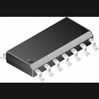
LMC6024IM National Semiconductor, LMC6024IM Datasheet

LMC6024IM
Specifications of LMC6024IM
Available stocks
Related parts for LMC6024IM
LMC6024IM Summary of contents
Page 1
... Specified for 100 kΩ and 5 kΩ loads n High voltage gain 120 dB n Low offset voltage drift 2.5 µV/˚C Connection Diagram © 2004 National Semiconductor Corporation n Ultra low input bias current Input common-mode range includes V n Operating range from +5V to +15V supply n Low distortion 0.01 kHz n Slew rate 0.11 V/µ ...
Page 2
... Absolute Maximum Ratings If Military/Aerospace specified devices are required, please contact the National Semiconductor Sales Office/ Distributors for availability and specifications. Differential Input Voltage + − Supply Voltage (V − Lead Temperature (Soldering, 10 sec.) Storage Temperature Range Voltage at Output/Input Pin (V Current at Input Pin Current at Output Pin ...
Page 3
DC Electrical Characteristics The following specifications apply for V face limits apply at the temperature extremes; all other limits T Symbol Parameter V Output Voltage Swing O I Output Current O I Supply Current S (Continued) + − = 5V, ...
Page 4
AC Electrical Characteristics The following specifications apply for V face limits apply at the temperature extremes; all other limits T Symbol Parameter SR Slew Rate GBW Gain-Bandwidth Product θ Phase Margin M G Gain Margin M Amp-to-Amp Isolation e Input-Referred ...
Page 5
Typical Performance Characteristics ± 7.5V 25˚C unless otherwise specified S A Supply Current vs Supply Voltage Common-Mode Voltage Range vs Temperature Output Characteristics Current Sourcing 01123527 Output Characteristics 01123529 01123531 5 Input Bias Current vs Temperature ...
Page 6
Typical Performance Characteristics Crosstalk Rejection vs Frequency CMRR vs Temperature Open-Loop Voltage Gain vs Temperature www.national.com ± 7.5V 25˚C unless otherwise specified (Continued 01123533 Power Supply Rejection 01123535 01123537 6 CMRR vs Frequency 01123534 ...
Page 7
Typical Performance Characteristics Gain and Phase Responses vs Load Capacitance Gain Error ( OUT Inverting Slew Rate vs Temperature ± 7.5V 25˚C unless otherwise specified (Continued Responses vs Temperature 01123539 ...
Page 8
Typical Performance Characteristics Non-Inverting Small Signal Pulse Response (A = +1) V Inverting Small-Signal Pulse Response Stability vs Capacitive Load www.national.com ± 7.5V 25˚C unless otherwise specified (Continued 01123545 Stability vs Capacitive Load 01123547 ...
Page 9
Application Hints AMPLIFIER TOPOLOGY The topology chosen for the LMC6024 is unconventional (compared to general-purpose op amps) in that the tradi- tional unity-gain buffer output stage is not used; instead, the output is taken directly from the output of the ...
Page 10
Application Hints (Continued) This would cause a 100 times degradation from the LMC6024’s actual performance. However guard ring is held within the inputs, then even a resistance of 10 ohms would cause only 0.05 pA ...
Page 11
Application Hints (Continued) (Input pins are lifted out of PC board and soldered directly to components. All other pins connected to PC board.) FIGURE 6. Air Wiring BIAS CURRENT TESTING The test method of Figure 7 is appropriate for bench-testing ...
Page 12
Typical Single-Supply Applications R5 R6, and R4 = R7; Then ∴ ≈ 100 for circuit shown For good CMRR over temperature, low drift resistors should be used. Matching and ...
Page 13
... High Gain Amplifier with Offset Voltage Reduction Gain = −46.8 Output offset voltage reduced to the level of the input offset voltage of the bottom amplifier (typically 1 mV), referred BIAS Ordering Information Temperature Range Industrial −40˚C ≤ LMC6024IM LMC6024IMX + ( (Continued) DC NSC Package Drawing ≤ +85˚C 14-Pin M14A Small Outline 13 ...
Page 14
... Deutsch Tel: +49 (0) 69 9508 6208 English www.national.com Français Tel: +33 ( 8790 14-Pin Small Outline Molded Package (M) Order Number LMC6024IM NS Package Number M14A 2. A critical component is any component of a life support device or system whose failure to perform can be reasonably expected to cause the failure of the life support device or system affect its safety or effectiveness ...


