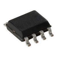
LMC6482IMM National Semiconductor, LMC6482IMM Datasheet - Page 17

LMC6482IMM
Manufacturer Part Number
LMC6482IMM
Description
IC, OP-AMP, 1.5MHZ, 1.3V/µs, MSOP-8
Manufacturer
National Semiconductor
Datasheet
1.LMC6482IMNOPB.pdf
(25 pages)
Specifications of LMC6482IMM
Op Amp Type
CMOS
No. Of Amplifiers
2
Bandwidth
1.5MHz
Slew Rate
1.3V/µs
Supply Voltage Range
3V To 15.5V
Amplifier Case Style
MSOP
No. Of Pins
8
Operating Temperature Range
-40°C To +85°C
Lead Free Status / RoHS Status
Contains lead / RoHS non-compliant
Available stocks
Company
Part Number
Manufacturer
Quantity
Price
Company:
Part Number:
LMC6482IMM
Manufacturer:
NS75
Quantity:
984
Part Number:
LMC6482IMM
Manufacturer:
NS/国半
Quantity:
20 000
Company:
Part Number:
LMC6482IMM/NOPB
Manufacturer:
National Semiconductor
Quantity:
25 066
Part Number:
LMC6482IMM/NOPB
Manufacturer:
TI/德州仪器
Quantity:
20 000
Company:
Part Number:
LMC6482IMMX
Manufacturer:
TI
Quantity:
168
Part Number:
LMC6482IMMX
Manufacturer:
NS/国半
Quantity:
20 000
Company:
Part Number:
LMC6482IMMX/NOPB
Manufacturer:
NS
Quantity:
17 500
Part Number:
LMC6482IMMX/NOPB
Manufacturer:
TI/德州仪器
Quantity:
20 000
Application Information
7.0 OFFSET VOLTAGE ADJUSTMENT
Offset voltage adjustment circuits are illustrated in Figure 12
Figure 13. Large value resistances and potentiometers are
used to reduce power consumption while providing typically
configurations with V
±
2.5mV of adjustment range, referred to the input, for both
FIGURE 13. Non-Inverting Configuration
FIGURE 12. Inverting Configuration
Offset Voltage Adjustment
Offset Voltage Adjustment
S
=
±
5V.
(Continued)
01171325
01171326
17
8.0 UPGRADING APPLICATIONS
The LMC6484 quads and LMC6482 duals have industry
standard pin outs to retrofit existing applications. System
performance can be greatly increased by the LMC6482’s
features. The key benefit of designing in the LMC6482 is
increased linear signal range. Most op-amps have limited
input common mode ranges. Signals that exceed this range
generate a non-linear output response that persists long
after the input signal returns to the common mode range.
Linear signal range is vital in applications such as filters
where signal peaking can exceed input common mode
ranges resulting in output phase inverison or severe distor-
tion.
9.0 DATA ACQUISITION SYSTEMS
Low power, single supply data acquisition system solutions
are provided by buffering the ADC12038 with the LMC6482
(Figure 14). Capable of using the full supply range, the
LMC6482 does not require input signals to be scaled down
to meet limited common mode voltage ranges. The
LMC4282 CMRR of 82dB maintains integral linearity of a
12-bit data acquisition system to
rail input amplifiers with only 50dB of CMRR will degrade the
accuracy of the data acquisition system to only 8 bits.
±
0.325 LSB. Other rail-to-
www.national.com


