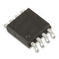
DAC101S101CIMM National Semiconductor, DAC101S101CIMM Datasheet

DAC101S101CIMM
Specifications of DAC101S101CIMM
Available stocks
Related parts for DAC101S101CIMM
DAC101S101CIMM Summary of contents
Page 1
... DAC081S101 and the 12-bit DAC121S101. The DAC101S101 operates over the extended industrial tem- perature range of −40˚C to +105˚C. Pin Configuration Ordering Information Order Numbers DAC101S101CIMM DAC101S101CIMMX DAC101S101CIMK DAC101S101CIMKX DAC101S101EVAL SPI ™ trademark of Motorola, Inc. © 2005 National Semiconductor Corporation ...
Page 2
Block Diagram Pin Descriptions TSOT MSOP (SOT-23) Pin No. Pin No www.national.com Symbol V DAC Analog Output Voltage. OUT GND Ground reference for all on-chip circuitry. ...
Page 3
... Absolute Maximum Ratings (Notes Military/Aerospace specified devices are required, please contact the National Semiconductor Sales Office/ Distributors for availability and specifications. Supply Voltage Voltage on any Input Pin Input Current at Any Pin (Note 3) Package Input Current (Note 3) Power Consumption 25˚C A ESD Susceptibility (Note 5) ...
Page 4
Electrical Characteristics Values shown in this table are design targets and are subject to change before product release. The following specifica- tions apply for V = +2.7V to +5.5V ≤ T Boldface limits apply for T MIN Symbol ...
Page 5
... Note 5: Human body model is 100 pF capacitor discharged through a 1.5 kΩ resistor. Machine model is 220 pF discharged through ZERO Ohms. Note 6: See the section entitled "Surface Mount" found in any post 1986 National Semiconductor Linear Data Book for methods of soldering surface mount devices. Note 7: The analog inputs are protected as shown below. Input voltage magnitudes However, errors in the conversion result can occur if any input goes above V ≤ ...
Page 6
Specification Definitions DIFFERENTIAL NON-LINEARITY (DNL) is the measure of the maximum deviation from the ideal step size of 1 LSB, which 1024 = V / 1024. REF A DIGITAL FEEDTHROUGH is a measure of the energy in- ...
Page 7
Transfer Characteristic FIGURE 1. Input / Output Transfer Characteristic Timing Diagram FIGURE 2. DAC101S101 Timing 7 20154105 20154106 www.national.com ...
Page 8
Typical Performance Characteristics unless otherwise stated DNL 3.0V A INL 3.0V A TUE 3.0V A www.national.com MHz 25C, Input Code Range 12 to 1011, SCLK A ...
Page 9
Typical Performance Characteristics unless otherwise stated (Continued) DNL vs DNL vs. f SCLK 3V DNL vs. Clock Duty Cycle MHz 25C, Input Code Range 12 to 1011, SCLK A 20154122 20154150 5V ...
Page 10
Typical Performance Characteristics unless otherwise stated (Continued) 3V DNL vs. Temperature 3V INL vs. f SCLK 3V INL vs. Clock Duty Cycle www.national.com MHz 25C, Input Code Range 12 to 1011, SCLK A 5V DNL ...
Page 11
Typical Performance Characteristics unless otherwise stated (Continued) 3V INL vs. Temperature Zero Code Error vs. f Zero Code Error vs. Temperature MHz, T SCLK 20154132 Zero Code Error vs. Clock Duty Cycle SCLK 20154134 20154136 11 = ...
Page 12
Typical Performance Characteristics unless otherwise stated (Continued) Full-Scale Error vs. Clock Duty Cycle Supply Current vs Glitch Response www.national.com MHz, T SCLK A Full-Scale Error vs. Temperature 20154138 Supply Current vs. Temperature A 20154144 20154146 ...
Page 13
Typical Performance Characteristics unless otherwise stated (Continued) 3V Wake-Up Time MHz 25C, Input Code Range 12 to 1011, SCLK A 5V Wake-Up Time 20154148 13 20154149 www.national.com ...
Page 14
Functional Description 1.1 DAC SECTION The DAC101S101 is fabricated on a CMOS process with an architecture that consists of switches and a resistor string that are followed by an output buffer. The power supply serves as the reference voltage. ...
Page 15
Functional Description was before entering power down. Minimum power consump- tion is achieved in the power-down mode with SCLK dis- abled and SYNC and D idled low. IN 2.0 Applications Information The simplicity of the DAC101S101 implies ease of ...
Page 16
Applications Information (Continued) FIGURE 9. The LM4130 as a power supply 2.2.2 LM4050 Available with accuracy of 0.44%, the LM4050 shunt refer- ence is also a good choice as a power regulator for the DAC101S101. It does not come ...
Page 17
Applications Information (Continued) num electrolytic capacitors are typically not a good choice due to their large size and have ESR values that may be too high at low temperatures. 2.3 BIPOLAR OPERATION The DAC101S101 is designed for single supply ...
Page 18
... Physical Dimensions unless otherwise noted www.national.com inches (millimeters) 8-Lead MSOP Order Numbers DAC101S101CIMM NS Package Number MUA08A 6-Lead TSOT Order Numbers DAC101S101CIMK NS Package Number MK06A 18 ...
Page 19
... BANNED SUBSTANCE COMPLIANCE National Semiconductor manufactures products and uses packing materials that meet the provisions of the Customer Products Stewardship Specification (CSP-9-111C2) and the Banned Substances and Materials of Interest Specification (CSP-9-111S2) and contain no ‘‘Banned Substances’’ as defined in CSP-9-111S2. ...


