LM3414HVSD National Semiconductor, LM3414HVSD Datasheet
LM3414HVSD
Specifications of LM3414HVSD
Available stocks


Related parts for LM3414HVSD


LM3414HVSD Summary of contents
Page 1
... The LM3414 and LM3414HV are available in ePSOP-8 and 3mm x 3mm LLP-8 packages. *Thermal de-rating applies according to actual operation con- ditions Simplified Application Schematic © 2010 National Semiconductor Corporation LM3414/LM3414HV Features ■ Support LED power up to 60W*: 18x 3W HBLEDs ■ ...
Page 2
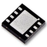
... Connection Diagram Ordering Information Order Number LM3414MR LM3414MRX LM3414HVMR LM3414HVMRX LM3414SD LM3414SDX LM3414HVSD LM3414HVSDX www.national.com Package Type NSC Package Drawing ePSOP-8 MRA08A LLP-8 SDA08AG 2 30124803 Supplied As 95 Units in Anti-Static Rails 2,500 Units on Tape and Reel 95 Units in Anti-Static Rails 2500 Units on Tape and Reel ...
Page 3
Pin Descriptions Pin(s) Name Description 1 VCC Internal Regulator Output Pin 2 PGND Power Ground Pin 3 IADJ Average Output Current Adjustment Pin 4 GND Analog Ground Pin 5 FS Switching Frequency Setting Pin 6 DIM PWM Dimming Control Pin ...
Page 4
... Absolute Maximum Ratings (LM3414) (Note 1) If Military/Aerospace specified devices are required, please contact the National Semiconductor Sales Office/ Distributors for availability and specifications. VIN to GND VIN to GND (Transient PGND LX to PGND (Transient) -3V(2 ns) to 45V (500 ms) FS, IADJ to GND DIM to GND ...
Page 5
... Absolute Maximum Ratings (LM3414HV) (Note 1) If Military/Aerospace specified devices are required, please contact the National Semiconductor Sales Office/ Distributors for availability and specifications. VIN to GND VIN to GND (Transient PGND LX to PGND (Transient) -3V(2 ns) to 67V (500 ms) FS, IADJ to GND DIM to GND ...
Page 6
Electrical Characteristics for +25°C (Note 4). Limits appearing in boldface type apply over full Operating Temperature Range. Datasheet min/max A J specification limits are obtained under device test mode and guaranteed by design, test, or statistical analysis. ...
Page 7
Symbol Parameter T Thermal Shutdown Temperature SD-HYS Hysteresis THERMAL RESISTANCE θ Junction to Ambient LFPM Air Flow (Note 3) Note 1: Absolute Maximum Ratings are limits beyond which damage to the device may occur. Operating Ratings are conditions ...
Page 8
Typical Performance Characteristics application for driving twelve power LEDs with LED) OUT IN LM3414HV Efficiency LED) IN LM3414HV I vs Temperature (T OUT (6 LED, V ...
Page 9
V vs Temperature ( LM3414HV I and V OUT LX LM3414HV LED Current with PWM Dimming (V DIM LM3414HV V IADJ 30124839 30124816 Rising) LED Current with PWM Dimming (V 30124856 9 vs Temperature ( ...
Page 10
LED Current with PWM Dimming (9µs dimming pulse), LM3414HV www.national.com 30124858 10 ...
Page 11
Block Diagram Operation Description OVERVIEW The LM3414/14HV is a high power floating buck LED driver with wide input voltage ranges. It requires no external current sensing elements and loop compensation networks. The in- tegrated power N-MOSFET enables high output power ...
Page 12
FIGURE 1. Switching Frequency (kHz) SW 250 500 1000 TABLE 1. Examples for f Settings SW To ensure accurate current regulation, the LM3414/14HV should be operated in continuous conduction mode (CCM) and the on time should not ...
Page 13
FIGURE 3. Waveforms of a Floating Buck LED Driver with PLM INDUCTOR SELECTION To ensure proper output current LM3414/14HV must operate in Continuous Conduction Mode (CCM). With the incorporation of PLM, the peak-to-peak in- ductor current ripple can be set ...
Page 14
PULSE-LEVEL-MODULATION (PLM) OPERATION PRINCIPLES The Pulse-Level-Modulation is a patented method to ensure accurate average output current regulation without the need of direct output current sensing. Figure 3 shows the current waveforms of a typical buck converter under steady state, where, ...
Page 15
FIGURE 5. Shortened Current Slew up Time of the LM3414/14HV To ensure normal operation of the LM3414/14HV rec- ommended to set the dimming frequency not higher than 1/10 of the switching frequency. The minimum dimming duty cycle is ...
Page 16
ANALOG DIMMING CONTROL The IADJ pin can be used as an analog dimming signal input. As the average output current of the LM3414 depends on the current being drawn from the IADJ pin, thus the LED current When external bias ...
Page 17
DESIGN EXAMPLE Figure 7 shows an example circuit for analog dimming control using simple external biasing circuitry with a variable resistor. FIGURE 7. Example Analog Dimming Control Circuit In the figure, the variable resistor VR1 controls the base volt- age ...
Page 18
Additional Application Circuit FIGURE 8. LM3414/14HV Design Example (I Designation Description U1 LED Driver IC LM3414 / LM3414HV L Inductor 47 µ Schottky Diode 100V 2. Cap MLCC 100V 2.2 µF X7R IN C Cap MLCC ...
Page 19
Physical Dimensions inches (millimeters) unless otherwise noted 8-Lead LLP Package NS Package Number SDA08A 8-Lead ePSOP Package NS Package Number MRA08B 19 www.national.com ...
Page 20
... For more National Semiconductor product information and proven design tools, visit the following Web sites at: www.national.com Products Amplifiers www.national.com/amplifiers Audio www.national.com/audio Clock and Timing www.national.com/timing Data Converters www.national.com/adc Interface www.national.com/interface LVDS www.national.com/lvds Power Management www.national.com/power Switching Regulators www.national.com/switchers LDOs www.national.com/ldo LED Lighting www ...