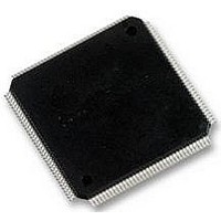
LFXP6C-5TN144C LATTICE SEMICONDUCTOR, LFXP6C-5TN144C Datasheet - Page 130

LFXP6C-5TN144C
Manufacturer Part Number
LFXP6C-5TN144C
Description
FPGA, 1.8V FLASH, INSTANT ON, SMD
Manufacturer
LATTICE SEMICONDUCTOR
Series
LatticeXPr
Datasheet
1.LFXP3C-3QN208C.pdf
(130 pages)
Specifications of LFXP6C-5TN144C
No. Of Logic Blocks
720
No. Of Macrocells
3000
Family Type
LatticeXP
No. Of Speed Grades
5
No. Of I/o's
100
Clock Management
PLL
Core Supply Voltage Range
1.71V To 3.465V
Lead Free Status / RoHS Status
Lead free / RoHS Compliant
Available stocks
Company
Part Number
Manufacturer
Quantity
Price
Company:
Part Number:
LFXP6C-5TN144C
Manufacturer:
LATTICE
Quantity:
2 291
Company:
Part Number:
LFXP6C-5TN144C
Manufacturer:
Lattice
Quantity:
60
Company:
Part Number:
LFXP6C-5TN144C
Manufacturer:
Lattice Semiconductor Corporation
Quantity:
10 000
Company:
Part Number:
LFXP6C-5TN144C-4I
Manufacturer:
LATTICE
Quantity:
2 291
Lattice Semiconductor
September 2005
September 2005
December 2005
December 2006
November 2007
February 2006
February 2007
August 2006
March 2006
March 2006
June 2006
April 2006
May 2006
July 2007
(cont.)
Date
Version
(cont.)
03.0
03.1
04.0
04.1
04.2
04.3
04.4
04.5
04.6
04.7
04.8
04.9
05.0
05.1
Characteristics (cont.)
Ordering Information
Pinout Information
Pinout Information
Pinout Information
Pinout Information
Pinout Information
Pinout Information
DC and Switching
DC and Switching
DC and Switching
DC and Switching
DC and Switching
DC and Switching
DC and Switching
DC and Switching
DC and Switching
Characteristics
Characteristics
Characteristics
Characteristics
Characteristics
Characteristics
Characteristics
Characteristics
Supplemental
Supplemental
Architecture
Architecture
Architecture
Introduction
Architecture
Architecture
Introduction
Information
Information
Section
Updated Typical Building Block Function Performance timing numbers.
Updated External Switching Characteristics timing numbers.
Updated Internal Timing Parameters.
Updated LatticeXP Family timing adders.
Updated LatticeXP "C" Sleep Mode timing numbers.
Updated JTAG Port Timing numbers.
Added clarification to SLEEPN and TOE description.
Clarification of dedicated LVDS outputs.
Updated list of technical notes.
Power Supply and NC Connections table corrected VCCP1 pin number
for 208 PQFP.
Moved data sheet from Advance to Final.
Added clarification to Typical I/O Behavior During Power-up section.
Added clarification to Recommended Operating Conditions.
Updated timing numbers.
Updated Signal Descriptions table.
Added clarification to Differential I/O Per Bank.
Updated Differential dedicated LVDS output support.
Added 208 PQFP lead-free package and ordering part numbers.
Corrected description of Signal Names VREF1(x) and VREF2(x).
Corrected condition for IIL and IIH.
Added clarification to Recommended Operating Conditions for
VCCAUX.
Removed Bank designator "5" from SLEEPN/TOE ball function.
Added footnote 2 regarding threshold level for PROGRAMN to sysCON-
FIG Port Timing Specifications table.
Corrected LVDS25E Output Termination Example.
Added clarification to Typical I/O Behavior During Power-Up section.
Added clarification to Left and Right sysIO Buffer Pair section.
Changes to LVDS25E Output Termination Example diagram.
EBR Asynchronous Reset section added.
Updated EBR Asynchronous Reset section.
Updated LatticeXP Family Selection Guide table.
Updated Typical I/O Behavior During Power-up text section.
Updated sysIO Single-Ended DC Electrical Characteristics table. Split
out LVCMOS 1.2 by supply voltage.
Added JTAG Port Timing Waveforms diagram.
Added Thermal Management text section.
Updated title list.
7-2
Change Summary
LatticeXP Family Data Sheet
Revision History


