IDT7133SA35JG INTEGRATED DEVICE TECHNOLOGY, IDT7133SA35JG Datasheet - Page 8
IDT7133SA35JG
Manufacturer Part Number
IDT7133SA35JG
Description
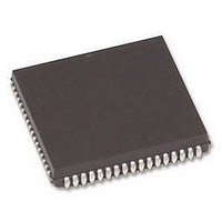
SRAM DUAL PORT 2KX16, 7133, PLCC68
Manufacturer
INTEGRATED DEVICE TECHNOLOGY
Datasheet
1.IDT7133SA35JG.pdf
(16 pages)
Specifications of IDT7133SA35JG
Memory Size
32Kbit
Access Time
35ns
Supply Voltage Range
4.5V To 5.5V
Memory Case Style
PLCC
No. Of Pins
68
Operating Temperature Range
0°C To +70°C
Operating Temperature Max
70°C
Operating
RoHS Compliant
Memory Configuration
2K X 16
Rohs Compliant
Yes


TIMING WAVEFORM OF READ CYCLE NO. 1, EITHER SIDE
TIMING WAVEFORM OF READ CYCLE NO. 2, EITHER SIDE
NOTES:
1. Timing depends on which signal is asserted last, OE or CE.
2. Timing depends on which signal is deasserted first, OE or CE.
3. t
4. Start of valid data depends on which timing becomes effective last, t
5. R/W = V
IDT7133SA/LA, IDT7143SA/LA
High-Speed 2K x 16 Dual-Port RAM
ADDRESS
relationship to valid output data.
BDD
DATA
CURRENT
BUSY
delay is required only in a case where the opposite port is completing a write operation to the same address location. For simultaneous read operations, BUSY has no
IH
OUT
OUT
DATA
, and the address is valid prior to or coincidental with CE transition LOW.
OUT
I
CE
OE
I
CC
SB
PREVIOUS DATA VALID
t
PU
t
OH
50%
AOE
t
, t
AA
ACE
t
LZ
, t
t
t
(1)
ACE
LZ
AA,
t
6.42
RC
t
(1)
AOE
8
or t
(4)
BDD
(4)
.
Military, Industrial and Commercial Temperature Ranges
(5)
(5)
t
BDD
(3,4)
DATA VALID
VALID DATA
t
OH
t
HZ
t
PD
(2)
t
HZ
50%
(2)
2746 drw 07
2746 drw 08
Related parts for IDT7133SA35JG
Image
Part Number
Description
Manufacturer
Datasheet
Request
R

Part Number:
Description:
HIGH-SPEED 2K x 16 CMOS DUAL-PORT STATIC RAMS
Manufacturer:
IDT [Integrated Device Technology]
Datasheet:

Part Number:
Description:
Integrated Processor
Manufacturer:
Integrated Device Technology, Inc.
Part Number:
Description:
Integrated Riscontroller for Low-Cost Systems
Manufacturer:
Integrated Device Technology, Inc.
Part Number:
Description:
INTEGRATED RISController FOR LOW-COST SYSTEMS
Manufacturer:
Integrated Device Technology, Inc.
Part Number:
Description:
SwitchStar ATM Cell Based 1.2Gbps non-blocking Integrated Switch Controller
Manufacturer:
Integrated Device Technology, Inc.
Datasheet:
Part Number:
Description:
3.3V CMOS 16-bit bidirectional transceiver
Manufacturer:
Integrated Device Technology, Inc.
Datasheet:
Part Number:
Description:
3.3 CMOS octal buffer/line driver
Manufacturer:
Integrated Device Technology, Inc.
Datasheet:
Part Number:
Description:
Fast CMOS octal registered transceivers
Manufacturer:
Integrated Device Technology, Inc.
Datasheet:
Part Number:
Description:
Fast CMOS octal bidirectional transceivers
Manufacturer:
Integrated Device Technology, Inc.
Datasheet:
Part Number:
Description:
Fast CMOS 16-bit buffer/line driver
Manufacturer:
Integrated Device Technology, Inc.
Datasheet:
Part Number:
Description:
2.5 V/3.3 V 10 Bit High Bandwidth Bus Switch with Precharged Outputs
Manufacturer:
Integrated Device Technology, Inc.
Datasheet:
Part Number:
Description:
High-Speed CMOS Quick Switch 16:8 Multiplexer
Manufacturer:
Integrated Device Technology, Inc.
Datasheet:
Part Number:
Description:
QUICKSWITCH?? PRODUCTS HIGH-SPEED CMOS QUICKSWITCH DOUBLE-WIDTH BUS SWITCH IDTQS32X245Q2QUICKSWITCH PRODUCTS HIGH-SPEED CMOS QUICKSWITCH DOUBLE-WIDTH BUS SWITCH
Manufacturer:
Integrated Device Technology, Inc.
Datasheet:
Part Number:
Description:
2.5V / 3.3V 16-BIT HIGH BANDWIDTH BUS SWITCH
Manufacturer:
Integrated Device Technology, Inc.
Datasheet:
Part Number:
Description:
QUICKSWITCH PRODUCTS 2.5V / 3.3V 8-BIT HIGH BANDWIDTH BUS SWITCH
Manufacturer:
Integrated Device Technology, Inc.
Datasheet: