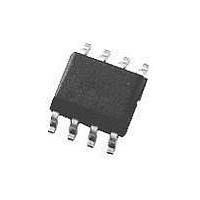
LM2594M-5.0 National Semiconductor, LM2594M-5.0 Datasheet - Page 9

LM2594M-5.0
Manufacturer Part Number
LM2594M-5.0
Description
IC, STEP-DOWN REGULATOR, 8-SOIC
Manufacturer
National Semiconductor
Datasheet
1.LM2594MX-5.0NOPB.pdf
(28 pages)
Specifications of LM2594M-5.0
Primary Input Voltage
12V
No. Of Outputs
1
Output Voltage
5V
Output Current
500mA
No. Of Pins
8
Operating Temperature Range
-40°C To +125°C
Supply Voltage Range
4.5V To 40V
Termination Type
SMD
Dc To Dc Converter Type
Inverting/Step Down
Number Of Outputs
1
Pin Count
8
Input Voltage
40V
Switching Freq
173kHz
Efficiency
82%
Package Type
SOIC N
Output Type
Fixed
Switching Regulator
Yes
Mounting
Surface Mount
Input Voltage (min)
4.5V
Operating Temp Range
-40C to 125C
Operating Temperature Classification
Automotive
Filter Terminals
SMD
Rohs Compliant
No
Input Voltage Primary Max
40V
Lead Free Status / RoHS Status
Contains lead / RoHS non-compliant
Lead Free Status / RoHS Status
Contains lead / RoHS non-compliant
Available stocks
Company
Part Number
Manufacturer
Quantity
Price
Company:
Part Number:
LM2594M-5.0
Manufacturer:
NS
Quantity:
5 000
Company:
Part Number:
LM2594M-5.0
Manufacturer:
NS
Quantity:
10
Part Number:
LM2594M-5.0
Manufacturer:
NS/国半
Quantity:
20 000
Company:
Part Number:
LM2594M-5.0/NOPB
Manufacturer:
TI
Quantity:
4 540
Company:
Part Number:
LM2594M-5.0/NOPB
Manufacturer:
NS
Quantity:
480
Part Number:
LM2594M-5.0/NOPB
Manufacturer:
NS/国半
Quantity:
20 000
LM2594/LM2594HV Series Buck Regulator Design Procedure (Fixed
Output)
Given:
V
V
I
1. Inductor Selection (L1)
A. Select the correct inductor value selection guide from Fig-
ures 4, 5 or Figure 6 . (Output voltages of 3.3V, 5V, or 12V re-
spectively.) For all other voltages, see the design procedure
for the adjustable version.
B. From the inductor value selection guide, identify the induc-
tance region intersected by the Maximum Input Voltage line
and the Maximum Load Current line. Each region is identified
by an inductance value and an inductor code (LXX).
C. Select an appropriate inductor from the four manufactur-
er’s part numbers listed in Figure 8 .
2. Output Capacitor Selection (C
A. In the majority of applications, low ESR (Equivalent Series
Resistance) electrolytic capacitors between 82 µF and
220 µF and low ESR solid tantalum capacitors between 15
µF and 100 µF provide the best results. This capacitor should
be located close to the IC using short capacitor leads and
short copper traces. Do not use capacitors larger than
220 µF.
For additional information, see section on output capaci-
tors in application information section.
B. To simplify the capacitor selection procedure, refer to the
quick design component selection table shown in Figure 2 .
This table contains different input voltages, output voltages,
and load currents, and lists various inductors and output ca-
pacitors that will provide the best design solutions.
C. The capacitor voltage rating for electrolytic capacitors
should be at least 1.5 times greater than the output voltage,
and often much higher voltage ratings are needed to satisfy
the low ESR requirements for low output ripple voltage.
D. For computer aided design software, see Switchers Made
Simple version 4.1 or later.
LOAD
OUT
IN
(max) = Maximum DC Input Voltage
(max) = Maximum Load Current
PROCEDURE (Fixed Output Voltage Version)
= Regulated Output Voltage (3.3V, 5V or 12V)
OUT
)
9
Given:
V
V
I
1. Inductor Selection (L1)
A. Use the inductor selection guide for the 5V version shown
in Figure 5 .
B. From the inductor value selection guide shown in Figure 5 ,
the inductance region intersected by the 12V horizontal line
and the 0.4A vertical line is 100 µH, and the inductor code is
L20.
C. The inductance value required is 100 µH. From the table
in Figure 8 , go to the L20 line and choose an inductor part
number from any of the four manufacturers shown. (In most
instance, both through hole and surface mount inductors are
available.)
2. Output Capacitor Selection (C
A. See section on output capacitors in application infor-
mation section.
B. From the quick design component selection table shown
in Figure 2 , locate the 5V output voltage section. In the load
current column, choose the load current line that is closest to
the current needed in your application, for this example, use
the 0.5A line. In the maximum input voltage column, select
the line that covers the input voltage needed in your applica-
tion, in this example, use the 15V line. Continuing on this line
are recommended inductors and capacitors that will provide
the best overall performance.
The capacitor list contains both through hole electrolytic and
surface mount tantalum capacitors from four different capaci-
tor manufacturers. It is recommended that both the manufac-
turers and the manufacturer’s series that are listed in the
table be used.
In this example aluminum electrolytic capacitors from several
different manufacturers are available with the range of ESR
numbers needed.
C. For a 5V output, a capacitor voltage rating at least 7.5V or
more is needed. But, in this example, even a low ESR,
switching grade, 120 µF 10V aluminum electrolytic capacitor
would exhibit approximately 400 m
in Figure 14 for the ESR vs voltage rating). This amount of
ESR would result in relatively high output ripple voltage. To
reduce the ripple to 1% of the output voltage, or less, a ca-
pacitor with a higher voltage rating (lower ESR) should be se-
lected. A 16V or 25V capacitor will reduce the ripple voltage
by approximately half.
LOAD
OUT
IN
(max) = 12V
120 µF 25V Panasonic HFQ Series
120 µF 25V Nichicon PL Series
(max) = 0.4A
= 5V
EXAMPLE (Fixed Output Voltage Version)
OUT
of ESR (see the curve
)
www.national.com


