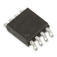
LM3881MM National Semiconductor, LM3881MM Datasheet

LM3881MM
Specifications of LM3881MM
Available stocks
Related parts for LM3881MM
LM3881MM Summary of contents
Page 1
... Time delays are defined using an external capac- itor and the output flag states can be inverted by the user. Typical Application Circuit © 2008 National Semiconductor Corporation Features ■ Easiest method to sequence rails ■ ...
Page 2
... Connection Diagram Ordering Information Order Number LM3881MM LM3881MMX Pin Descriptions Pin # www.national.com Top View MSOP-8 Package Package Type NSC Package Drawing MSOP-8 MUA08A Name VCC EN GND INV TADJ FLAG3 FLAG2 FLAG1 2 30048402 Supplied As 1000 Units on Tape and Reel 3500 Units on Tape and Reel ...
Page 3
... Absolute Maximum Ratings If Military/Aerospace specified devices are required, please contact the National Semiconductor Sales Office/ Distributors for availability and specifications. VCC, EN, INV, TADJ, FLAG1, FLAG2, FLAG3 to GND Storage Temperature Range Junction Temperature Lead Temperature (Soldering, 5 sec.) Minimum ESD Rating (Note 2) Electrical Characteristics apply over the full Operating Temperature Range (T test, design or statistical correlation ...
Page 4
Typical Performance Characteristics Quiescent Current vs V Enable Threshold vs Temperature Time Delay vs Temperature ( Nominal) ADJ www.national.com V = 3.3V unless otherwise specified. CC Quiescent Current vs Temperature CC 30048414 30048416 30048418 4 30048415 Time ...
Page 5
FLAG Voltage vs Current 30048420 5 www.national.com ...
Page 6
Block Diagram www.national.com 6 30048403 ...
Page 7
Application Information OVERVIEW The LM3881 Power Sequencer provides a simple solution for sequencing multiple rails in a controlled manner. A clock sig- nal is established that facilitates control of the power up and power down of three open drain FET ...
Page 8
FIGURE 2. Power Up Sequence, INV Low FIGURE 3. Power Up Sequence, INV High 8 30048425 30048405 ...
Page 9
FIGURE 4. Power Down Sequence, INV Low FIGURE 5. Power Down Sequence, INV High 9 30048406 30048424 www.national.com ...
Page 10
ENABLE CIRCUIT The enable circuit is designed with an internal comparator, referenced to a bandgap voltage (1.22V), to provide a preci- sion threshold. This allows the timing to be set externally using a capacitor as shown in the diagram below. ...
Page 11
FIGURE 10. Incomplete Sequence Timing, INV Low 11 30048412 30048413 www.national.com ...
Page 12
Physical Dimensions www.national.com inches (millimeters) unless otherwise noted MSOP-8 Package NS Package Number MUA08A 12 ...
Page 13
Notes 13 www.national.com ...
Page 14
... For more National Semiconductor product information and proven design tools, visit the following Web sites at: Products Amplifiers www.national.com/amplifiers Audio www.national.com/audio Clock Conditioners www.national.com/timing Data Converters www.national.com/adc Displays www.national.com/displays Ethernet www.national.com/ethernet Interface www.national.com/interface LVDS www.national.com/lvds Power Management www.national.com/power Switching Regulators www.national.com/switchers LDOs www ...


