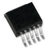
LP3964ES-3.3 National Semiconductor, LP3964ES-3.3 Datasheet - Page 16

LP3964ES-3.3
Manufacturer Part Number
LP3964ES-3.3
Description
V REG ULTRA-LDO +3.3V, SMD, 3964
Manufacturer
National Semiconductor
Datasheet
1.LP3964ES-3.3.pdf
(22 pages)
Specifications of LP3964ES-3.3
Primary Input Voltage
4.3V
Output Voltage
3.3V
Dropout Voltage Vdo
240mV
No. Of Pins
5
Output Current
800mA
Voltage Regulator Case Style
TO-263
Operating Temperature Range
-40°C To +125°C
Output Voltage Fixed
3.3V
Rohs Compliant
Yes
Lead Free Status / RoHS Status
Lead free / RoHS Compliant
www.national.com
Application Hints
HEATSINKING TO-263 AND SOT-223 PACKAGES
The TO-263 and SOT223 packages use the copper plane on
the PCB as a heatsink. The tab of these packages are
soldered to the copper plane for heat sinking. Figure 3
shows a curve for the θ
copper area sizes, using a typical PCB with 1 ounce copper
and no solder mask over the copper area for heat sinking.
As shown in the figure, increasing the copper area beyond 1
square inch produces very little improvement. The minimum
value for θ
32˚C/W.
Figure 4 shows the maximum allowable power dissipation
for TO-263 packages for different ambient temperatures,
assuming θ
ture is 125˚C.
Figure 5 shows a curve for the θ
different copper area sizes, using a typical PCB with 1 ounce
copper and no solder mask over the copper area for heat
sinking.
FIGURE 3. θ
FIGURE 4. Maximum power dissipation vs ambient
JA
JA
temperature for TO-263 package
for the TO-263 packag mounted to a PCB is
is 35˚C/W and the maximum junction tempera-
JA
vs Copper(1 Ounce) Area for TO-263
JA
package
of TO-263 package for different
(Continued)
JA
of SOT-223 package for
10112932
10112933
16
The following figures show different layout scenarios for
SOT-223 package.
FIGURE 5. θ
FIGURE 6. SCENARIO A, θ
FIGURE 7. SCENARIO B, θ
JA
vs Copper(1 Ounce) Area for SOT-223
package
JA
JA
= 148˚C/W
= 125˚C/W
10112919
10112921
10112920


