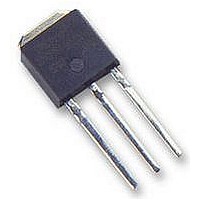
XC6216D502JR Torex Semiconductor Ltd, XC6216D502JR Datasheet - Page 20

XC6216D502JR
Manufacturer Part Number
XC6216D502JR
Description
LDO 5.0V OUTPUT, CMOS 28V, TO252
Manufacturer
Torex Semiconductor Ltd
Datasheet
1.XC6216B302MR.pdf
(43 pages)
Specifications of XC6216D502JR
Primary Input Voltage
7V
Output Voltage
5V
Dropout Voltage Vdo
300mV
No. Of Pins
3
Output Current
150mA
Voltage Regulator Case Style
TO-252
Operating Temperature Range
-40°C To +85°C
Svhc
No
Output Voltage Fixed
5V
Rohs Compliant
Yes
Lead Free Status / RoHS Status
Lead free / RoHS Compliant
Available stocks
Company
Part Number
Manufacturer
Quantity
Price
Part Number:
XC6216D502JR
Manufacturer:
TOREX
Quantity:
20 000
20/43
■ OPERATIONAL EXPLANATION
<Output Voltage Control>
<Short-Circuit Protection>
The XC6216/XE6216 series includes a current fold-back circuit as a short circuit protection. When the load current reaches
the current limit level, the current fold-back circuit operates and output voltage drops. The output voltage drops further and
output current decreases. When the output pin is shorted, a current of about 30mA flows.
<CE Pin>
The IC’s internal circuitry can be shutdown via the signal from the CE pin with the XC6216/XE6216 series. In shutdown
mode, output at the V
is ‘High Active/No pull down’, operations will become unstable with the CE pin open. We suggest that you use this IC with
either a V
operational logic is fixed and the IC will operate normally. However, supply current may increase as a result of through
current in the IC’s internal circuitry if a medium voltage is applied.
<Thermal Shutdown>
When the junction temperature of the built-in driver transistor reaches the temperature limit level (150℃ TYP.), the thermal
shutdown circuit operates and the driver transistor will be set to OFF. The IC resumes its operation when the thermal
shutdown function is released and the IC’s operation is automatically restored because the junction temperature drops to the
level of the thermal shutdown release voltage.
<Minimum Operating Voltage>
For the stable operation of the IC, over 2.0V of input voltage is necessary. The output voltage may not be generated
normally if the input voltage is less than 2.0V.
XC6216/XE6216
The voltage divided by resistors R11 & R12 is compared with the internal reference voltage by the error amplifier. The
P-channel MOSFET which is connected to the V
voltage at the V
protect circuit operate in relation to the level of output current and heat dissipation. Further, the IC’s internal circuitry
can be shutdown via the CE pin’s signal.
IN
voltage or a V
OUT
OUT
pin is controlled and stabilized by a system of negative feedback. The current limit circuit and short
pin will be pulled down by R11 and R12 to the V
SS
voltage input at the CE pin. If this IC is used with the correct specifications for the CE pin, the
Series
OUT
pin is then driven by the subsequent output signal. The output
SS
level. Note that as the XC6216/XE6216 series


