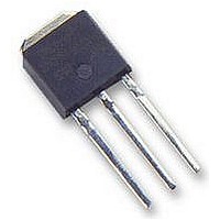
XC6216D502JR Torex Semiconductor Ltd, XC6216D502JR Datasheet - Page 21

XC6216D502JR
Manufacturer Part Number
XC6216D502JR
Description
LDO 5.0V OUTPUT, CMOS 28V, TO252
Manufacturer
Torex Semiconductor Ltd
Datasheet
1.XC6216B302MR.pdf
(43 pages)
Specifications of XC6216D502JR
Primary Input Voltage
7V
Output Voltage
5V
Dropout Voltage Vdo
300mV
No. Of Pins
3
Output Current
150mA
Voltage Regulator Case Style
TO-252
Operating Temperature Range
-40°C To +85°C
Svhc
No
Output Voltage Fixed
5V
Rohs Compliant
Yes
Lead Free Status / RoHS Status
Lead free / RoHS Compliant
Available stocks
Company
Part Number
Manufacturer
Quantity
Price
Part Number:
XC6216D502JR
Manufacturer:
TOREX
Quantity:
20 000
■ NOTES ON USE
1. Please use this IC within the stated absolute maximum ratings. The IC is liable to malfunction should the ratings be
2. Where wiring impedance is high, operations may become unstable due to the noise and/or phase lag depending on output
3. Phase compensation inside the IC is performed in the XC6216/XE6216 series. Therefore, an abnormal oscillation does not
4. Notes on Setting Output Voltage Externally (C type) Ta=25℃
●Setting Resistance-Dependant of XC6216 Series’ Output Voltage
The output voltage can be set externally by the following equation:
If the equation (3) is assigned to the equation (2), the equation becomes as below:
For this, the following equation can be used for setting output voltage externally:
And the equation (4) will be;
The second term of the equation (6), R
The I
The cause of the output accuracy error, R
Accordingly, if R
exceeded.
current. Please strengthen V
occur even if there is no output capacitor C
V
because of the load change can be controlled by placing the output capacitor CL around 0.1uF~1.0uF between the V
pin and V
with a shorter wiring.
SS
FB
pin is required for input stability. Also, the output voltage fluctuation such as under shoot or over shoot, which occurs
can be calculated by the following equation:
I
I
I
V
V
V
I
R
21
22
21
FB
SS
OUT
OUT
OUT
21
=I
=2.0V/R
=I
=2.0V / R
・
pin. The input capacitor (C
FB
FB
I
=2.0V
=2.0V+R
=2.0V+R
=2.0V+R
FB
21
+I
+2.0V/R
=2.0V
=R
<< R
22
21
22
・
・
FB
FB
(R
・
21
21
2.0V/ R
, the output voltage error becomes minute.
21
22
21
R
・
・
21
・
+ R
I
I
21
21
(I
/ R
FB
22
FB
IN
FB
+2.0V/R
) / R
and V
22
21
+ R
・
SS
22
21
I
IN
)
・
21
FB
wiring in particular.
) and the output capacitor (C
・
, is the cause of the output accuracy error.
I
FB
L
. An input capacitor C
I
FB
can be calculated by the equation below;
………………………………………………………………………
………………………………………………………………………
………………………………………………………………………
………………………………………………………………………
………………………………………………………………………
………………………………………………………………………
………………………………………………………………………
………………………………………………………………………
………………………………………………………………………
IN
around 0.1uF~1.0uF between the V
L
) should be placed to the IC as close as possible
XC6216/XE6216
IN
pin and the
21/43
Series
(1)
(2)
(3)
(4)
(5)
(6)
(7)
OUT


