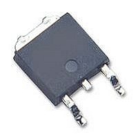
LP2954IS National Semiconductor, LP2954IS Datasheet - Page 5

LP2954IS
Manufacturer Part Number
LP2954IS
Description
IC, LDO VOLT REG, 5V, 250mA, TO-263
Manufacturer
National Semiconductor
Datasheet
1.LP2954AIT.pdf
(15 pages)
Specifications of LP2954IS
Primary Input Voltage
30V
Output Voltage Fixed
5V
Dropout Voltage Vdo
800mV
No. Of Pins
3
Output Current
250mA
Operating Temperature Range
-40°C To +125°C
Termination Type
SMD
Lead Free Status / RoHS Status
Contains lead / RoHS non-compliant
Available stocks
Company
Part Number
Manufacturer
Quantity
Price
Electrical Characteristics
Note 1: Absolute maximum ratings indicate limits beyond which damage to the component may occur. Electrical specifications do not apply when operating the
device outside of its rated operating conditions.
Note 2: The maximum allowable power dissipation is a function of the maximum junction temperature, T
and the ambient temperature, T
.
Exceeding the maximum allowable power dissipation will result in excessive die temperature, and the regulator will go into thermal shutdown. The junction-to-
ambient thermal resistance of the TO-220 (without heatsink) is 60˚C/W, 73˚C/W for the TO-263, and 160˚C/W for the SO-8. If the TO-263 package is used, the
thermal resistance can be reduced by increasing the P.C. board copper area thermally connected to the package: Using 0.5 square inches of copper area, θ
50˚C/W; with 1 square inch of copper area, θ
is 3˚C/W. If an external heatsink is used, the effective junction-to-ambient thermal resistance is the sum of the junction-to-case resistance (3˚C/W), the specified
thermal resistance of the heatsink selected, and the thermal resistance of the interface between the heatsink and the LP2954. Some typical values are listed for
interface materials used with TO-220:
Note 3: Output voltage temperature coefficient is defined as the worst case voltage change divided by the total temperature range.
Note 4: Regulation is measured at constant junction temperature using low duty cycle pulse testing. Parts are tested separately for load regulation in the load
ranges 0.1 mA–1 mA and 1 mA–250 mA. Changes in output voltage due to heating effects are covered by the thermal regulation specification.
Note 5: Dropout voltage is defined as the input to output differential at which the output voltage drops 100 mV below the value measured with a 1V differential.
Note 6: Ground pin current is the regulator quiescent current. The total current drawn from the source is the sum of the load current plus the ground pin current.
Note 7: Thermal regulation is defined as the change in output voltage at a time T after a change in power dissipation is applied, excluding load or line regulation
effects. Specifications are for 200 mA load pulse at V
Note 8: When used in dual-supply systems where the regulator load is returned to a negative supply, the output voltage must be diode-clamped to ground.
Note 9: Connect a 0.1µF capacitor from the output to the feedback pin.
Note 10: V
Note 11: Two seperate tests are performed, one covering V
Note 12: V
Note 13: Comparator thresholds are expressed in terms of a voltage differential at the Feedback terminal below the nominal reference voltage measured at
V
Note 14: Human body model, 200pF discharged through 1.5kΩ.
Typical Performance Characteristics
IN
Thermal Resistance (˚C/W) (Data from AAVID Eng.)
=V
O
TABLE 1. Typical Values of Case-to-Heatsink
(NOM)+1V. To express these thresholds in terms of output voltage change, multiply by the Error amplifier gain, which is V
REF
SHUTDOWN
Silicone grease
Dry interface
Mica with grease
≤V
OUT
≤(V
≤1.1V, VOUT=V
IN
Quiescent Current
−1V), 2.3V≤V
A
. The maximum allowable power dissipation at any ambient temperature is calculated using:
O
(NOM).
IN
≤30V, 100µA≤I
JA
is 37˚C/W; and with 1.6 or more square inches of copper area, θ
IN
(Continued)
= 20V (3W pulse) for T = 10 ms.
1.0
1.3
1.4
01112812
L
≤250mA.
IN
=2.5V to V
O
(NOM)+1V and the other test for V
5
Thermal Resistance (˚C/W) (Data from Thermalloy)
TABLE 2. Typical Values of Case-to-Heatsink
Thermasil III
Thermasil II
Thermalfilm (0.002) with grease
J
(MAX), the junction-to-ambient thermal resistance, θ
JA
IN
Quiescent Current
=2.5V to V
is 32˚C/W. The junction-to-case thermal resistance
O
(NOM)+1V to 30V.
OUT
/V
REF
=(R1+R2)/R2.
01112813
1.3
1.5
2.2
www.national.com
JA
J-A
is
,


