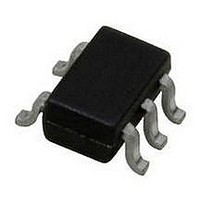
LM94022QBIMG/NOPB National Semiconductor, LM94022QBIMG/NOPB Datasheet - Page 5

LM94022QBIMG/NOPB
Manufacturer Part Number
LM94022QBIMG/NOPB
Description
IC TEMP SENSOR ± 1.5°C TO ± 2.7°C SC70-5
Manufacturer
National Semiconductor
Datasheet
1.LM94022EVAL.pdf
(16 pages)
Specifications of LM94022QBIMG/NOPB
Ic Output Type
Voltage
Sensing Accuracy Range
± 2.7°C
Supply Current
5.4µA
Supply Voltage Range
1.5V To 5.5V
Sensor Case Style
SC-70
No. Of Pins
5
Msl
MSL 1 - Unlimited
Lead Free Status / RoHS Status
Lead free / RoHS Compliant
I
C
V
V
I
I
S
IH
IL
IH
IL
L
Electrical Characteristics
Unless otherwise noted, these specifications apply for +V
T
Note 1: Absolute Maximum Ratings indicate limits beyond which damage to the device may occur. Operating Ratings indicate conditions for which the device is
functional, but do not guarantee specific performance limits. For guaranteed specifications and test conditions, see the Electrical Characteristics. The guaranteed
specifications apply only for the test conditions listed. Some performance characteristics may degrade when the device is not operated under the listed test
conditions.
Note 2: When the input voltage (V
Note 3: The human body model is a 100 pF capacitor discharged through a 1.5 kΩ resistor into each pin. The machine model is a 200 pF capacitor discharged
directly into each pin.
Note 4: Reflow temperature profiles are different for lead-free and non-lead-free packages.
Note 5: The junction to ambient thermal resistance (θ
Note 6: Typicals are at T
Note 7: Limits are guaranteed to National's AOQL (Average Outgoing Quality Level).
Note 8: Accuracy is defined as the error between the measured and reference output voltages, tabulated in the Transfer Table at the specified conditions of
supply gain setting, voltage, and temperature (expressed in °C). Accuracy limits include line regulation within the specified conditions. Accuracy limits do not
include load regulation; they assume no DC load.
Note 9: Changes in output due to self heating can be computed by multiplying the internal dissipation by the thermal resistance.
Note 10: Source currents are flowing out of the LM94022. Sink currents are flowing into the LM94022.
Note 11: Line regulation (DC) is calculated by subtracting the output voltage at the highest supply voltage from the output voltage at the lowest supply voltage.
The typical DC line regulation specification does not include the output voltage shift discussed in Section 5.0.
Note 12: Guaranteed by design and characterization.
Note 13: The input current is leakage only and is highest at high temperature. It is typically only 0.001µA. The 1µA limit is solely based on a testing limitation and
does not reflect the actual performance of the part.
Symbol
MAX
; all other limits T
Sensor Gain
Load Regulation
(Note 10)
Line Regulation
(Note 11)
Supply Current
Output Load Capacitance
Power-on Time (Note 12)
GS1 and GS0 Input Logic
"1" Threshold Voltage
GS1 and GS0 Input Logic
"0" Threshold Voltage
Logic "1" Input Current
(Note 13)
Logic "0" Input Current
(Note 13)
J
Parameter
= T
A
A
= T
= 25°C and represent most likely parametric norm.
I
J
) at any pin exceeds power supplies (V
= 25°C.
GS1 = 0, GS0 = 0
GS1 = 0, GS1 = 1
GS1 = 1, GS0 = 0
GS1 = 1, GS0 = 1
Source
(V
Sink
V
T
(V
T
(V
C
JA
OUT
A
A
L
DD
DD
DD
= 0 pF to 1100 pF
) is specified without a heat sink in still air.
= +30°C to +150°C,
= -50°C to +150°C,
≤
- V
- V
- V
≥
50 μA,
≤
200mV
OUT
OUT
OUT
50 μA,
Conditions
)
)
)
≥
≥
≥
DD
200mV
100mV
100mV
I
= +1.5V to +5.5V. Boldface limits apply for T
< GND or V
5
I
> V
+
), the current at that pin should be limited to 5 mA.
(Note 6)
Typical
0.001
0.001
-10.9
-13.6
-0.22
1100
0.26
-5.5
-8.2
200
5.4
5.4
0.7
Limits (Note 7)
V
DD
8.1
1.9
0.5
-1
- 0.5V
1
9
1
1
A
= T
J
= T
www.national.com
MIN
mV (max)
mV (max)
ms (max)
μA (max)
μA (max)
pF (max)
μA (max)
μA (max)
to
V (max)
V (min)
(Limit)
mV/°C
mV/°C
mV/°C
mV/°C
Units
μV/V


