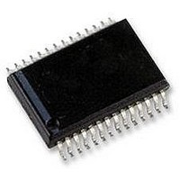
DS92LV1224TMSA National Semiconductor, DS92LV1224TMSA Datasheet

DS92LV1224TMSA
Specifications of DS92LV1224TMSA
Available stocks
Related parts for DS92LV1224TMSA
DS92LV1224TMSA Summary of contents
Page 1
... The DS92LV1224 was designed with the flow-through pinout and is available in a space saving 28–lead SSOP package. Block Diagrams TRI-STATE ® registered trademark of National Semiconductor Corporation. © 2005 National Semiconductor Corporation Features n 30–66 MHz Single 1:10 Deserializer with 300–660 Mb/s troughput ...
Page 2
Block Diagrams (Continued) Functional Description The DS92LV1224 is a 10-bit Deserializer device which to- gether with a compatible serializer (i.e. DS92LV1023E) forms a chipset designed to transmit data over FR-4 printed circuit board backplanes and balanced copper cables at clock ...
Page 3
Data Transfer (Continued) clock and uses it to recover the serialized data. ROUT data is valid when LOCK is low. Otherwise ROUT0–ROUT9 is invalid. The ROUT0-ROUT9 pins use the RCLK pin as the reference to data. The polarity of the ...
Page 4
... Ordering Information NSID DS92LV1224TMSA DIN0 Held Low-DIN1 Held High Creates an RMT Pattern DIN4 Held Low-DIN5 Held High Creates an RMT Pattern FIGURE 1. RMT Patterns Seen on the Bus LVDS Serial Output www.national.com Function Deserializer 20138724 DIN8 Held Low-DIN9 Held High Creates an RMT Pattern ...
Page 5
... Absolute Maximum Ratings If Military/Aerospace specified devices are required, please contact the National Semiconductor Sales Office/ Distributors for availability and specifications. Supply Voltage ( LVCMOS/LVTTL Input Voltage −0. LVCMOS/LVTTL Output Voltage −0. Bus LVDS Receiver Input Voltage Junction Temperature Storage Temperature Lead Temperature ...
Page 6
Deserializer Timing Requirements for REFCLK Over recommended operating supply and temperature ranges unless otherwise specified. Symbol Parameter t REFCLK Period RFCP t REFCLK Duty Cycle RFDC t / Ratio of REFCLK to RFCP t TCLK TCP t REFCLK Transition Time ...
Page 7
Deserializer Switching Characteristics Over recommended operating supply and temperature ranges unless otherwise specified. Symbol Parameter Conditions Deserializer PLL Lock t DSR2 time from SYNCPAT TRI-STATE to HIGH t ZHLK Delay (power-up) Deserializer Noise Figure 10 t RNM Margin (Note 7) ...
Page 8
AC Timing Diagrams and Test Circuits www.national.com (Continued) FIGURE 4. SYNC Timing Delays FIGURE 5. Deserializer Delay 8 20138723 20138712 ...
Page 9
AC Timing Diagrams and Test Circuits Timing shown for RCLK_R/F = LOW Duty Cycle ( RDC FIGURE 7. Deserializer TRI-STATE Test Circuit and Timing (Continued) FIGURE 6. Deserializer Data Valid Out Times 9 20138713 20138714 www.national.com ...
Page 10
AC Timing Diagrams and Test Circuits FIGURE 8. Deserializer PLL Lock Times and PWRDN TRI-STATE Delays FIGURE 9. Deserializer PLL Lock Time from SyncPAT www.national.com (Continued) 10 20138715 20138722 ...
Page 11
AC Timing Diagrams and Test Circuits SW - Setup and Hold Time (Internal Data Sampling Window Serializer Output Bit Position Jitter that results from Jitter on TCLK DJIT t = Receiver Noise Margin Time RNM FIGURE 10. Receiver ...
Page 12
Application Information USING THE SERIALIZER AND DESERIALIZER CHIPSET The Serializer and Deserializer chipset is an easy to use transmitter and receiver pair that sends 10 bits of parallel LVTTL data over a serial Bus LVDS link up to 660 Mbps. ...
Page 13
Application Information USING T AND T TO VALIDATE SIGNAL DJIT RNM QUALITY The parameters t and t can be used to generate an DJIT RNM eye pattern mask to validate signal quality in an actual application or in simulation. The ...
Page 14
... PWRDN I LOCK O RCLK O REN I www.national.com FIGURE 13. Random Lock Hot Insertion DS92LV1224TMSA - Deserializer 20138719 No. ± 15–19, 24–28 Data Output CMOS level outputs. 2 Recovered Clock Rising/Falling strobe select. TTL level input. Selects RCLK active edge for strobing of ROUT data. High selects rising edge. Low selects falling edge. ...
Page 15
Deserializer Pin Description Pin Name I/O DVCC I DGND I AVCC I AGND I REFCLK I (Continued) No. 21, 23 Digital Circuit power supply. 14, 20, 22 Digital Circuit ground Analog power supply (PLL and Analog Circuits). 1, ...
Page 16
... Tel: 1-800-272-9959 Deutsch Tel: +49 (0) 69 9508 6208 English www.national.com Français Tel: +33 ( 8790 Order Number DS92LV1224TMSA NS Package Number MSA28 2. A critical component is any component of a life support device or system whose failure to perform can be reasonably expected to cause the failure of the life support device or system affect its safety or effectiveness ...


