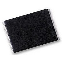
HY27UF082G2B-TPCB HYNIX SEMICONDUCTOR, HY27UF082G2B-TPCB Datasheet - Page 3

HY27UF082G2B-TPCB
Manufacturer Part Number
HY27UF082G2B-TPCB
Description
IC, MEMORY, FLASH NAND 2GB, TSOP48
Manufacturer
HYNIX SEMICONDUCTOR
Datasheet
1.HY27UF082G2B-TPCB.pdf
(54 pages)
Specifications of HY27UF082G2B-TPCB
Access Time
20ns
Supply Voltage Range
2.7V To 3.6V
Memory Case Style
TSOP
No. Of Pins
48
Operating Temperature Range
0°C To +70°C
Package / Case
TSOP
Base Number
27
Interface
Serial
Logic
RoHS Compliant
Memory Type
Flash - NAND
Memory Configuration
256M X 8
Rohs Compliant
Yes
Available stocks
Company
Part Number
Manufacturer
Quantity
Price
Company:
Part Number:
HY27UF082G2B-TPCB
Manufacturer:
PANASONIC
Quantity:
1 200
Company:
Part Number:
HY27UF082G2B-TPCB
Manufacturer:
HYNIX
Quantity:
2 526
Company:
Part Number:
HY27UF082G2B-TPCB
Manufacturer:
HY
Quantity:
744
Company:
Part Number:
HY27UF082G2B-TPCB
Manufacturer:
HYNIX
Quantity:
10 554
Part Number:
HY27UF082G2B-TPCB
Manufacturer:
HYNIX/海力士
Quantity:
20 000
Rev 0.2 / Jan. 2008
FEATURES SUMMARY
HIGH DENSITY NAND FLASH MEMORIES
- Cost effective solutions for mass storage applications
MULTIPLANE ARCHITECTURE
NAND INTERFACE
- x8/x16 bus width.
- Address/ Data Multiplexing
- Pinout compatiblity for all densities
SUPPLY VOLTAGE
- 3.3V device : Vcc = 2.7 V ~3.6 V
MEMORY CELL ARRAY
- x8 : (2K + 64) bytes x 64 pages x 2048 blocks
- x16 : (1K + 32) words x 64 pages x 2048 blocks
PAGE SIZE
- (2K + 64 spare) Bytes
- (1K + 32 spare) Words
BLOCK SIZE
- (128K + 4Kspare) Bytes
- (64K + 2Kspare) Words
PAGE READ / PROGRAM
- Random access : 25us (max.)
- Sequential access : 25ns (min.)
- Page program time : 200us (typ.)
- Multi-page program time (2 pages) : 200us (typ.)
COPY BACK PROGRAM
- Automatic block download without latency time
FAST BLOCK ERASE
- Block erase time: 1.5ms (typ.)
- Multi-block erase time (2 blocks) : 1.5ms (typ.)
CACHE READ
- Internal (2048 + 64) Byte buffer to improve the read
- Array is split into two independent planes. Parallel
throughtput.
Operations on both planes are available, halving
Program and erase time.
STATUS REGISTER
- Normal Status Register (Read/Program/Erase)
- Extended Status Register (EDC)
ELECTRONIC SIGNATURE
- 1st cycle : Manufacturer Code
- 2nd cycle : Device Code
- 3rd cycle : Internal chip number, Cell Type, Number of
- 4th cycle : Page size, Block size, Organization, Spare
- 5th cycle : Multiplane information
CHIP ENABLE DON’T CARE
- Simple interface with microcontroller
HARDWARE DATA PROTECTION
- Program/Erase locked during Power transitions.
DATA RETENTION
- 100,000 Program/Erase cycles (with 1bit/528byte ECC)
- 10 years Data Retention
PACKAGE
- HY27UF(08/16)2G2B-T(P)
- HY27UF082G2B-UP
- HY27UF082G2B-F(P)
: 63-Ball FBGA (9 x 11 x 1.0 mm)
2Gbit (256Mx8bit) NAND Flash
- HY27UF082G2B-F (Lead)
- HY27UF082G2B-FP (Lead Free)
: 52-ULGA (12 x 17 x 0.65 mm)
- HY27UF082G2B-UP (Lead Free)
: 48-Pin TSOP1 (12 x 20 x 1.2 mm)
Simultaneously Programmed Pages.
- HY27UF(08/16)2G2B-T (Lead)
- HY27UF(08/16)2G2B-TP (Lead Free)
size
HY27UF(08/16)2G2B Series
3


