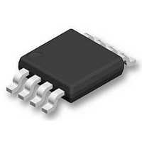
LMH6622MM National Semiconductor, LMH6622MM Datasheet - Page 14

LMH6622MM
Manufacturer Part Number
LMH6622MM
Description
IC, OP AMP, DUAL 160MHZ, POWERWISE
Manufacturer
National Semiconductor
Datasheet
1.LMH6622MMNOPB.pdf
(17 pages)
Specifications of LMH6622MM
Op Amp Type
Wideband
No. Of Amplifiers
2
Bandwidth
160MHz
Slew Rate
85V/µs
Supply Voltage Range
± 2.25V To ± 6V
Amplifier Case Style
MSOP
No. Of Pins
8
Operating Temperature Range
-40°C To
Lead Free Status / RoHS Status
Lead free / RoHS Compliant
Available stocks
Company
Part Number
Manufacturer
Quantity
Price
Part Number:
LMH6622MM
Manufacturer:
NS/国半
Quantity:
20 000
Part Number:
LMH6622MM/NOPB
Manufacturer:
TI/德州仪器
Quantity:
20 000
Part Number:
LMH6622MMX/NOPB
Manufacturer:
TI/德州仪器
Quantity:
20 000
www.national.com
DSL Receive Channel Applications
The two R
ing through the 1:N transformer.
Where R
The resistors R
the pre-amp. The receive gain is selected to meet the ADC
full-scale requirement of a DSL chipset.
Resistor R
cancellation of the output driver signal at the output of the
receiver.
Since the LMH6622 is configured as an inverting summing
amplifier, V
The expression for V
position principle.
When V
When V
Therefore,
And then,
Setting R
receive path, then we have
We can also find that,
And then
In conclusion, the peak-to-peak voltage to the ADC would
be,
(Continued)
S
A
L
N is the turns ratio of the transformer.
1
= 0,
= 0,
S
is the impedance of the twisted pair line.
1
OUT
= 2*R
resistors are used to provide impedance match-
and R
2
is found to be,
and R
2
to cancel unwanted driver signal in the
2
1
along with R
and V
F
are used to set the receive gain of
2
can be found by using super-
F
are used to achieve
14
RECEIVE CHANNEL NOISE CALCULATION
The circuit of Figure 2 also has the characteristic that it
cancels noise power from the drive channel.
The noise gain of the receive pre-amp is found to be:
Noise power at each of the output of LMH6622:
where
For a voltage feedback amplifier,
Therefore, total output noise from the differential pre-amp is:
The factor ’2 ’ appears here because of differential output.
DIFFERENTIAL ANALOG-TO-DIGITAL DRIVER
V
i
i
i
k
T
R
n
non-inv
inv
n
+
FIGURE 3. Circuit for Differential A/D Driver
Input referred voltage noise
Input referred current noise
Input referred non-inverting current noise
Input referred inverting current noise
Boltzmann’s constant, K = 1.38 x 10
Resistor temperature in k
Source resistance at the non-inverting input
to balance offset voltage, typically very small
for this inverting summing applications
−23
20029239


