SAK-C164CI-8E25M Infineon Technologies, SAK-C164CI-8E25M Datasheet
SAK-C164CI-8E25M
Specifications of SAK-C164CI-8E25M
Available stocks


Related parts for SAK-C164CI-8E25M


SAK-C164CI-8E25M Summary of contents
Page 1
Microcomputer Components 16-Bit CMOS Single-Chip Microcontroller C164CI Data Sheet 02.98 Preliminary ...
Page 2
C164CI Revision History: Previous Releases: Page Subjects 3, 4 Alternate functions for P5 added. 25...30 Register Table updated 32, 33 and P6H P6L 33, 34 Supply current specification improved. 33, 34 Idle supply current specification 39, 40 ADC ...
Page 3
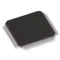
... Packages, Emulators, Evaluation Boards, HLL-Debuggers, Simulators, Logic Analyzer Disassemblers, Programming Boards On-Chip Bootstrap Loader 80-Pin MQFP Package, 0.65 mm pitch This document describes the SAF-C164CI-8EM and the SAK-C164CI-8EM. For simplicity all versions are referred to by the term C164CI throughout this document. Semiconductor Group 16 bit Division (32/16 bit) ...
Page 4
Introduction The C164CI is a new low cost derivative of the Siemens C166 Family of 16-bit single-chip CMOS microcontrollers. It combines high CPU performance ( million instructions per second) with high peripheral functionality and enhanced IO-capabilities. It also ...
Page 5
Pin Configuration (top view AREF P5.4/AN4/T2EUD 2 P5.5/AN5/T4EUD 3 P5.6/AN6/T2IN 4 P5.7/AN7/T4IN P3.4/T3EUD 8 P3.6/T3IN 9 P3.8/MRST 10 P3.9/MTSR 11 P3.10/TxD0 12 P3.11/RxD0 13 P3.12/BHE/WRH 14 P3.13/SCLK 15 P3.15/CLKOUT 16 P4.0/A16/CS3 ...
Page 6
Pin Definitions and Functions Symbol Pin Input (I) Number Output (O) P5.0 – 79 P3.4, 8, I/O P3.6, 9, I/O P3.8 – 10 – I/O P3.13, 15, I/O P3.15 16 I/O ...
Page 7
Pin Definitions and Functions (cont’d) Symbol Pin Input (I) Number Output ( WRL ALE PORT0: I/O P0L.0 – P0L.7, 36 P0H 39, P0H.7 ...
Page 8
Pin Definitions and Functions (cont’d) Symbol Pin Input (I) Number Output (O) PORT1: I/O P1L.0 – 52, P1L. P1H.0 - 59, P1H I I I/O ...
Page 9
Pin Definitions and Functions (cont’d) Symbol Pin Input (I) Number Output (O) RSTOUT 70 O NMI 71 I P8.0 – I/O P8.3 75 I/O 72 I/O ... ... 75 I AREF AGND ...
Page 10
Functional Description The C164CI is a low cost downgrade of the high performance microcontroller C167CR with OTP or internal ROM, reduced peripheral functionality and a high performance Capture Compare Unit with an additional functionality. The architecture of the C164CI combines ...
Page 11
Memory Organization The memory space of the C164CI is configured in a Von Neumann architecture which means that code memory, data memory, registers and I/O ports are organized within the same linear address space which includes 4 MBytes. The entire ...
Page 12
Central Processing Unit (CPU) The main core of the CPU consists of a 4-stage instruction pipeline, a 16-bit arithmetic and logic unit (ALU) and dedicated SFRs. Additional hardware has been spent for a separate multiply and divide unit, a bit-mask ...
Page 13
The CPU disposes of an actual register context consisting wordwide GPRs which are physically allocated within the on-chip RAM area. A Context Pointer (CP) register determines the base address of the active register bank to be ...
Page 14
Interrupt System With an interrupt response time within a range from just 250 ns to 600 ns (in case of internal program execution), the C164CI is capable of reacting very fast to the occurrence of non- deterministic events. The architecture ...
Page 15
Source of Interrupt or PEC Service Request GPT1 Timer 4 A/D Conversion Complete A/D Overrun Error ASC0 Transmit ASC0 Receive ASC0 Error SSC Transmit SSC Receive SSC Error CAPCOM Register 16 CAPCOM Register 17 CAPCOM Register 18 CAPCOM Register 19 ...
Page 16
The C164CI also provides an excellent mechanism to identify and to process exceptions or error conditions that arise during run-time, so-called ‘Hardware Traps’. Hardware traps cause immediate non-maskable system reaction which is similar to a standard interrupt service (branching to ...
Page 17
The Capture/Compare Unit CAPCOM2 The general purpose CAPCOM2 unit supports generation and control of timing sequences channels with a maximum resolution of 400 ns (at 20 MHz system clock). The CAPCOM units are typically used to ...
Page 18
The Capture/Compare Unit CAPCOM6 The CAPCOM6 unit supports generation and control of timing sequences three 16-bit capture/compare channels plus one 10-bit compare channel. In compare mode the CAPCOM6 unit provides two output signals per channel which have ...
Page 19
General Purpose Timer (GPT) Unit The GPT unit represents a very flexible multifunctional timer/counter structure which may be used for many different time related tasks such as event timing and counting, pulse width and duty cycle measurements, pulse generation, or ...
Page 20
Figure 6 GPT Block Diagram Watchdog Timer The Watchdog Timer represents one of the fail-safe mechanisms which have been implemented to prevent the controller from malfunctioning for longer periods of time. The Watchdog Timer is always enabled after a reset ...
Page 21
Real Time Clock The Real Time Clock (RTC) module of the C164CI consists of a chain of 3 divider blocks, a fixed 8- bit divider, the reloadable 16-bit timer T14 and the 32-bit RTC timer (accessible via registers RTCH and ...
Page 22
A/D Converter For analog signal measurement, a 10-bit A/D converter with 8 multiplexed input channels and a sample and hold circuit has been integrated on-chip. It uses the method of successive approximation. The sample time (for loading the capacitors) and ...
Page 23
Serial Channels Serial communication with other microcontrollers, processors, terminals or external peripheral components is provided by two serial interfaces with different functionality, an Asynchronous/ Synchronous Serial Channel (ASC0) and a High-Speed Synchronous Serial Channel (SSC). The ASC0 is upward compatible ...
Page 24
CAN-Module The integrated CAN-Module handles the completely autonomous transmission and reception of CAN frames in accordance with the CAN specification V2.0 part B (active), ie. the on-chip CAN- Module can receive and transmit standard frames with 11-bit identifiers as well ...
Page 25
Instruction Set Summary The table below lists the instructions of the C164CI in a condensed way. The various addressing modes that can be used with a specific instruction, the operation of the instructions, parameters for conditional execution of instructions, and ...
Page 26
Instruction Set Summary (cont’d) Mnemonic MOV(B) MOVBS MOVBZ JMPA, JMPI, JMPR JMPS J(N)B JBC JNBS CALLA, CALLI, CALLR CALLS PCALL TRAP PUSH, POP SCXT RET RETS RETP RETI SRST IDLE PWRDN SRVWDT DISWDT EINIT ATOMIC EXTR EXTP(R) EXTS(R) NOP Semiconductor ...
Page 27
Special Function Registers Overview The following table lists all SFRs which are implemented in the C164CI in alphabetical order. Bit-addressable SFRs are marked with the letter “b” in column “Name”. SFRs within the Extended SFR-Space (ESFRs) are marked with the ...
Page 28
Name Physical 8-Bit Address Address CC16 FE60 30 H CC16IC b F160 CC17 FE62 31 H CC17IC b F162 CC18 FE64 32 H CC18IC b F164 CC19 FE66 33 H CC19IC ...
Page 29
Name Physical 8-Bit Address Address DP0H b F102 DP0L b F100 DP1H b F106 DP1L b F104 DP3 b FFC6 E3 H DP4 b FFCA E5 H DP8 ...
Page 30
Name Physical 8-Bit Address Address P1L b FF04 FFC4 FFC8 FFA2 D1 H P5DIDIS b FFA4 FFD4 EA H PECC0 FEC0 60 H PECC1 ...
Page 31
Name Physical 8-Bit Address Address SSCCON b FFB2 D9 H SSCEIC b FF76 BB H SSCRB F0B2 SSCRIC b FF74 BA H SSCTB F0B0 SSCTIC b FF72 B9 H STKOV FE14 0A H STKUN ...
Page 32
Name Physical 8-Bit Address Address T8REL F056 TFR b FFAC D6 H TRCON b FF34 9A H UAR EFn2 X --- H WDT FEAE 57 H WDTCON b FFAE D7 H XP0IC b F186 ...
Page 33
... Absolute Maximum Ratings Ambient temperature under bias ( T SAF-C164CI ................................................................................................................ –40 to +85 °C SAK-C164CI .............................................................................................................. –40 to +125 °C Storage temperature ( T )........................................................................................ – +150 °C ST Voltage on V pins with respect to ground ( V DD Voltage on any pin with respect to ground ( V Input current on any pin during overload condition.................................................... –10 to +10 mA Absolute sum of all input currents during overload condition ...
Page 34
... V = 4. -40 to +85 °C for SAF-C164CI -40 to +125 °C for SAK-C164CI A Parameter Input low voltage (TTL) Input low voltage (Special Threshold) Input high voltage, all except RSTIN and XTAL1 (TTL) Input high voltage RSTIN Input high voltage XTAL1 Input high voltage ...
Page 35
Parameter XTAL1 input current 5) Pin capacitance (digital inputs/outputs) Power supply current (active) with all peripherals active Idle mode supply current with all peripherals active Idle mode supply current with all peripherals deactivated, PLL off, SDD factor = 32 Power-down ...
Page 36
Figure 7 Active and Idle Supply Current as a Function of Operating Frequency 1500 1250 1000 750 500 250 4 Figure 8 Idle and Power Down Supply Current as a Function of Oscillator Frequency Semiconductor Group ...
Page 37
AC Characteristics Definition of Internal Timing The internal operation of the C164CI is controlled by the internal CPU clock f CPU clock can trigger internal (eg. pipeline) or external (eg. bus cycles) operations. The specification of the external timing (AC ...
Page 38
C164CI Clock Generation Modes P0.15-13 CPU Frequency (P0H.7- CPU XTAL XTAL XTAL XTAL ...
Page 39
Phase Locked Loop For all other combinations of pins P0.15-13 (P0H.7-5) during reset the on-chip phase locked loop is enabled and provides the CPU clock (see table above). The PLL multiplies the input frequency by the factor F which is ...
Page 40
... AC Characteristics External Clock Drive XTAL1 4. -40 to +85 °C for SAF-C164CI -40 to +125 °C for SAK-C164CI A Parameter Symbol Oscillator period t OSC High time t 1 Low time t 2 Rise time t 3 Fall time The minimum and maximum oscillator periods for PLL operation depend on the selected CPU clock generation mode ...
Page 41
... A/D Converter Characteristics 4. -40 to +85 °C for SAF-C164CI -40 to +125 °C for SAK-C164CI AREF DD Parameter Analog input voltage range Basic clock frequency Conversion time Total unadjusted error Internal resistance of reference voltage source Internal resistance of analog source ADC input capacitance Sample time and conversion time of the C164CI’ ...
Page 42
Notes 1) V may exceed AIN AGND AREF cases will be X000 or X3FF The limit values for f must not be exceeded when selecting the CPU frequency and the ADCTC setting ...
Page 43
Testing Waveforms AC inputs during testing are driven at 2.4 V for a logic ‘1’ and 0.45 V for a logic ‘0’. Timing measurements are made at Figure 12 Input Output Waveforms For timing purposes a port pin is no ...
Page 44
... Multiplexed Bus V = 4. -40 to +85 °C for SAF-C164CI -40 to +125 °C for SAK-C164CI A C (for PORT0, PORT1, Port 4, ALE, RD, WR, BHE, CLKOUT) = 100 ALE cycle time = 6 TCL + 2 Parameter ALE high time Address setup to ALE Address hold after ALE ALE falling edge to RD, ...
Page 45
Parameter RD to valid data in (no RW-delay) ALE low to valid data in Address to valid data in Data hold after RD rising edge Data float after RD Data valid to WR Data hold after WR ALE rising edge ...
Page 46
Parameter RdCS, WrCS Low Time (with RW delay) RdCS, WrCS Low Time (no RW delay) Data valid to WrCS Data hold after RdCS Data float after RdCS Address hold after RdCS, WrCS Data hold after WrCS Semiconductor Group Symbol Max. ...
Page 47
ALE CSx A23-A16 (A15-A8) BHE t Read Cycle BUS RD RdCSx Write Cycle BUS WR, WRL, WRH WrCSx Figure 14-1 External Memory Cycle: Multiplexed Bus, With Read/Write Delay, Normal ALE Semiconductor Group ...
Page 48
ALE t 38 CSx A23-A16 (A15-A8) BHE t 6 Read Cycle BUS RD RdCSx Write Cycle BUS WR, WRL, WRH WrCSx Figure 14-2 External Memory Cycle: Multiplexed Bus, With Read/Write Delay, Extended ALE Semiconductor Group ...
Page 49
ALE CSx A23-A16 (A15-A8) BHE t Read Cycle BUS RD RdCSx Write Cycle BUS WR, WRL, WRH WrCSx Figure 14-3 External Memory Cycle: Multiplexed Bus, No Read/Write Delay, Normal ALE Semiconductor Group ...
Page 50
ALE t 38 CSx A23-A16 (A15-A8) BHE t 6 Read Cycle BUS RD RdCSx Write Cycle BUS WR, WRL, WRH WrCSx Figure 14-4 External Memory Cycle: Multiplexed Bus, No Read/Write Delay, Extended ALE Semiconductor Group ...
Page 51
... AC Characteristics CLKOUT 4. -40 to +85 °C for SAF-C164CI -40 to +125 °C for SAK-C164CI A C (for PORT0, PORT1, Port 4, ALE, RD, WR, BHE, CLKOUT) = 100 pF L Parameter Symbol t CLKOUT cycle time t CLKOUT high time t CLKOUT low time t CLKOUT rise time CLKOUT fall time ...
Page 52
CLKOUT ALE Command RD, WR Figure 15 CLKOUT Timing Notes 1) Cycle as programmed, including MCTC waitstates (Example shows 0 MCTC WS). 2) The leading edge of the respective command depends on RW-delay. 3) Multiplexed bus modes have a MUX ...
Page 53
Package Outline Plastic Package, P-MQFP-80-1 (SMD) (Plastic Metric Quad Flat Package) 0.65 0.3 ±0. Index Marking 1) Does not include plastic or metal protrusions of 0.25 max per side Figure 16 Sorts of Packing Package outlines for ...