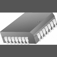
DP8573AV National Semiconductor, DP8573AV Datasheet - Page 11

DP8573AV
Manufacturer Part Number
DP8573AV
Description
Clock IC
Manufacturer
National Semiconductor
Datasheet
1.DP8573AV.pdf
(16 pages)
Specifications of DP8573AV
Date Format
BCD
Clock Format
12 Or 24 Hr
Clock Ic Type
RTC
Digital Ic Case Style
LCC
No. Of Pins
28
Peak Reflow Compatible (260 C)
No
Supply Voltage Max
5.5V
Leaded Process Compatible
No
Mounting Type
Surface Mount
Lead Free Status / RoHS Status
Contains lead / RoHS non-compliant
Available stocks
Company
Part Number
Manufacturer
Quantity
Price
Company:
Part Number:
DP8573AV
Manufacturer:
NSC
Quantity:
5 510
Part Number:
DP8573AV
Manufacturer:
NS/国半
Quantity:
20 000
Company:
Part Number:
DP8573AV/NOPB
Manufacturer:
Renesas
Quantity:
207
Company:
Part Number:
DP8573AV/NOPB
Manufacturer:
Texas Instruments
Quantity:
10 000
Functional Description
MAIN STATUS REGISTER
The Main Status Register is always located at address 0
regardless of the register block selected
D0 This read only bit is a general interrupt status bit that is
taken directly from the interrupt pins The bit is a one when
an interrupt is pending on either the INTR pin or the MFO
pin (when configured as an interrupt) This is unlike D3
which can be set by an internal event but may not cause an
interrupt This bit is reset when the interrupt status bits in the
Main Status Register are cleared
D1 –D3 These three bits of the Main Status Register are the
main interrupt status bits Any bit may be a one when any of
the interrupts are pending Once an interrupt is asserted the
interrupt status bits are not reset when read Except for D1
to reset an interrupt a one is written back to the correspond-
ing bit that is being tested D1 is reset whenever the PFAIL
pin
reading the register in a polled mode D1 and D3 are set
regardless of whether these interrupts are masked or not by
bits D6 and D7 of Interrupt Control Registers 0 and 1
D4 D5 and D7 General purpose RAM bits
D6 Bit D6 controls the register block to be accessed (see
memory map)
PERIODIC FLAG REGISTER
The Periodic Flag Register has the same bit for bit corre-
spondence as Interrupt Control Register 0 except for D6
and D7 For normal operation (i e not a single supply appli-
cation) this register must be written to on initial power up or
after an oscillator fail event D0–D5 are read only bits D6
and D7 are read write
D0 –D5 These bits are set by the real time rollover events
(Time Change
read and can be used as selective data change flags
D6 This bit performs a dual function When this bit is read a
one indicates that an oscillator failure has occurred and the
time information may have been lost Some of the ways an
oscillator failure might be caused are failure of the crystal
shorting OSC IN or OSC OUT to GND or V
crystal removal of battery when in the battery backed mode
(when a ‘‘0’’ is written to D6) lowering the voltage at the
V
BB
P will read this register to determine the cause These
e
pin to a value less than 2 2V when in the battery
logic 1 This prevents loss of interrupt status when
e
1) The bits are reset when the register is
(Continued)
CC
TL F 9981 – 12
TL F 9981 – 13
removal of
11
backed mode Bit D6 is automatically set to 1 on initial pow-
er-up or an oscillator fail event The oscillator fail flag is
reset by writing a one to the clock start stop bit in the Real
Time Mode Register with the crystal oscillating
When D6 is written to it defines whether the TCP is being
used in battery backed (normal) or in a single supply mode
application When set to a one this bit configures the TCP
for single power supply applications This bit is automatically
set on initial power-up or an oscillator fail event When set
D6 disables the oscillator reference circuit The result is that
the oscillator is referenced to V
D6 the oscillator reference is enabled thus the oscillator is
referenced to V
standby applications
At initial power on if the DP8573A is going to be pro-
grammed for battery backed mode the V
connected to a potential in the range of 2 2V to V
0 4V
For single supply mode operation the V
connected to GND and the PFAIL pin connected to V
D7 Writing a one to this bit enables the test mode register
at location 1F (see Table III) This bit should be forced to
zero during initialization for normal operation If the test
mode has been entered clear the test mode register before
leaving test mode (See separate test mode application
note for further details )
TIME SAVE CONTROL REGISTER
D0– D5 General purpose RAM bits
D6 Not Available appears as logic 0 when read
D7 Time Save Enable bit controls the loading of real-time-
clock data into the Time Save RAM When a one is written
to this bit the Time Save RAM will follow the corresponding
clock registers and when a zero is written to this bit the time
in the Time Save RAM is frozen This eliminates any syn-
chronization problems when reading the clock thus negat-
ing the need to check for a counter rollover during a read
cycle
This bit must be set to a one prior to power failing to enable
the Time Save feature When the power fails this bit is auto-
matically reset and the time is saved in the Time Save RAM
REAL TIME MODE REGISTER
BB
This allows operation in standard battery
CC
When a zero is written to
BB
BB
pin should be
pin should be
TL F 9981 – 14
TL F 9981 – 15
CC
CC
b


