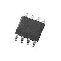
DS90C402M National Semiconductor, DS90C402M Datasheet - Page 3

DS90C402M
Manufacturer Part Number
DS90C402M
Description
LVDS Line Receiver IC
Manufacturer
National Semiconductor
Specifications of DS90C402M
No. Of Drivers
2
Driver Case Style
NSOIC
No. Of Pins
8
Mounting Type
Surface Mount
No. Of Driver/receivers
2/0
Peak Reflow Compatible (260 C)
No
Supply Voltage
5V
Supply Voltage Max
5V
Lead Free Status / RoHS Status
Contains lead / RoHS non-compliant
Available stocks
Company
Part Number
Manufacturer
Quantity
Price
Company:
Part Number:
DS90C402M
Manufacturer:
ns
Quantity:
2 602
Part Number:
DS90C402M
Manufacturer:
NS/国半
Quantity:
20 000
Company:
Part Number:
DS90C402M/NOPB
Manufacturer:
NSC
Quantity:
650
Part Number:
DS90C402MX
Manufacturer:
NS/国半
Quantity:
20 000
Company:
Part Number:
DS90C402MX/NOPB
Manufacturer:
ACTEL
Quantity:
210
Part Number:
DS90C402MX/NOPB
Manufacturer:
TI/德州仪器
Quantity:
20 000
Parameter Measurement Information
Typical Application
Applications Information
LVDS drivers and receivers are intended to be primarily used
in an uncomplicated point-to-point configuration as is shown
in Figure 3. This configuration provides a clean signaling
environment for the quick edge rates of the drivers. The
receiver is connected to the driver through a balanced media
which may be a standard twisted pair cable, a parallel pair
cable, or simply PCB traces. Typically the characteristic
impedance of the media is in the range of 100Ω. A termina-
tion resistor of 100Ω should be selected to match the media,
and is located as close to the receiver input pins as possible.
The termination resistor converts the current sourced by the
driver into a voltage that is detected by the receiver. Other
configurations are possible such as a multi-receiver configu-
ration, but the effects of a mid-stream connector(s), cable
stub(s), and other impedance discontinuities as well as
ground shifting, noise margin limits, and total termination
loading must be taken into account.
The DS90C402 differential line receiver is capable of detect-
ing signals as low as 100 mV, over a
range centered around +1.2V. This is related to the driver
FIGURE 1. Receiver Propagation Delay and Transition Time Test Circuit
FIGURE 2. Receiver Propagation Delay and Transition Time Waveforms
±
1V common-mode
FIGURE 3. Point-to-Point Application
3
offset voltage which is typically +1.2V. The driven signal is
centered around this voltage and may shift
center point. The
potential difference between the driver’s ground reference
and the receiver’s ground reference, the common-mode ef-
fects of coupled noise, or a combination of the two. Both
receiver input pins should honor their specified operating
input voltage range of 0V to +2.4V (measured from each pin
to ground), exceeding these limits may turn on the ESD
protection circuitry which will clamp the bus voltages.
Fail-Safe Feature:
The LVDS receiver is a high gain, high speed device that
amplifies a small differential signal (20mV) to CMOS logic
levels. Due to the high gain and tight threshold of the re-
ceiver, care should be taken to prevent noise from appearing
as a valid signal.
The receiver’s internal fail-safe circuitry is designed to
source/sink a small amount of current, providing fail-safe
protection (a stable known state HIGH output voltage) for
floating, terminated or shorted receiver inputs.
10000604
±
1V shifting may be the result of a ground
10000605
10000608
±
1V around this
www.national.com


