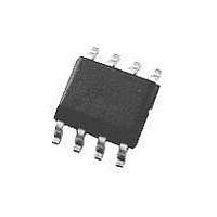
LM3485MM National Semiconductor, LM3485MM Datasheet

LM3485MM
Specifications of LM3485MM
Available stocks
Related parts for LM3485MM
LM3485MM Summary of contents
Page 1
... The cycle-by-cycle current limit can be ad- justed with a single resistor, ensuring safe operation over a range of output currents. Features n Easy to use control methodology n No control loop compensation required Typical Application Circuit © 2004 National Semiconductor Corporation n 4.5V to 35V wide input range n 1.242V High Efficiency 93% ± ± ...
Page 2
... Connection Diagram Package Marking and Ordering Information Order Number LM3485MM LM3485MMX Pin Description Pin Name Pin Number ISENSE GND NC FB ADJ PWR GND PGATE VIN www.national.com Top View 20034609 8 Lead Plastic MSOP-8 NS package Number MUA08A Package Type Package Marking MSOP-8 S29B ...
Page 3
... Absolute Maximum Ratings If Military/Aerospace specified devices are required, please contact the National Semiconductor Sales Office/ Distributors for availability and specifications. VIN Voltage PGATE Voltage FB Voltage ISENSE Voltage ADJ Voltage Maximum Junction Temp. Power Dissipation Electrical Characteristics Specifications in Standard type face are for T Range (T = − ...
Page 4
Electrical Characteristics Specifications in Standard type face are for T Range (T = −40˚C to +125˚C). Unless otherwise specified min/max specification limits are guaranteed by design, test, or statistical analysis. Symbol Parameter % Feedback Voltage FB ...
Page 5
Typical Performance Characteristics Quiescent Current vs Input Voltage (FB = 1.5V) Hysteresis Voltage vs Input Voltage Current Limit ADJ Current vs Temperature Unless otherwise specified, T Feedback Voltage vs Temperature 20034601 Hysteresis Voltage vs Temperature 20034605 Current Limit One Shot ...
Page 6
Typical Performance Characteristics PGATE Voltage vs Input Voltage Minimum ON Time vs. Temperature Operating ON Time vs Output Load Current (V = 12V) IN www.national.com Unless otherwise specified, T Typical V 20034603 Operating ON Time vs Output Load Current 20034612 ...
Page 7
Typical Performance Characteristics Efficiency vs Load Current (V = 3.3V 22µH) OUT Start Up Discontinuous Mode Operation (V = 12V 50mA 22µH) IN OUT OUT Unless otherwise specified, T Efficiency vs ...
Page 8
Typical Performance Characteristics Output Ripple Voltage vs Input Voltage (V = 3.3V 1A, C OUT OUT OUT(ESR) Feed-Forward Capacitor (Cff) Effect (V = 3.3V 22µH, I OUT www.national.com Unless otherwise specified 80m , C ...
Page 9
Block Diagram Functional Description OVERVIEW The LM3485 is buck (step-down) DC-DC controller that uses a hysteretic control scheme. The comparator is designed with approximately 10mV of hysteresis. In response to the voltage at the FB pin, the gate drive (PGATE ...
Page 10
Functional Description The minimum output voltage ripple (V lated in the same way OUT_PP HYST For example, with V set to 3.3V, V OUT V = 0.01* ( 33K + ...
Page 11
Functional Description 20034626 FIGURE 4. Current Limit Fold Back Phenomenon > At high input voltages ( 28V) increased undershoot at the switch node can cause an increase in the current limit threshold. To avoid this problem, a low Vf Schottky ...
Page 12
Design Information Hysteretic control is a simple control scheme. However the operating frequency and other performance characteristics highly depend on external conditions and components. If either the inductance, output capacitance, ESR, V changed, there will be a change in the ...
Page 13
Design Information (Continued − D) D_AVE OUT The off state voltage across the catch diode is approximately equal to the input voltage. The peak reverse voltage rating must be greater than input voltage. In nearly ...
Page 14
PCB Layout (Continued) FIGURE 6. Typical PCB Layout Schematic (3.3V output) www.national.com 20034628 14 ...
Page 15
PCB Layout (Continued) Top Layer C1: C 22µF/35V EEJL1VD226R (Panasonic) IN C2: C 100µF/6.3V 6TPC100M (Sanyo) OUT C3: C 1nF Ceramic Chip Capacitor ADJ C4: C 100pF Ceramic Chip Capacitor FF D1: 1A/40V MBRS140T3 (On Semiconductor) L1: 22µH :QH66SN220M01L (Murata) ...
Page 16
... BANNED SUBSTANCE COMPLIANCE National Semiconductor certifies that the products and packing materials meet the provisions of the Customer Products Stewardship Specification (CSP-9-111C2) and the Banned Substances and Materials of Interest Specification (CSP-9-111S2) and contain no ‘‘Banned Substances’’ as defined in CSP-9-111S2. ...


