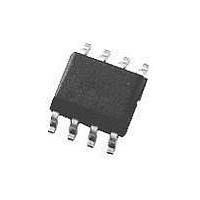
LM7121IM National Semiconductor, LM7121IM Datasheet

LM7121IM
Specifications of LM7121IM
Available stocks
Related parts for LM7121IM
LM7121IM Summary of contents
Page 1
... Low supply current: 5.3 mA Applications n Scanners, color fax, digital copiers n PC video cards n Cable drivers n Digital cameras n ADC/DAC buffers n Set-top boxes DS012348-2 NSC Drawing Package Number Marking M08A LM7121IM M08A LM7121IM MA05A A03A MA05A A03A August 1999 = ± 15V S 175 MHz = +1, R ...
Page 2
... Absolute Maximum Ratings If Military/Aerospace specified devices are required, please contact the National Semiconductor Sales Office/ Distributors for availability and specifications. ESD Tolerance (Note 2) Differential Input Voltage (Note 7) Voltage at Input/Output Pin (V + − Supply Voltage (V –V ) Output Short Circuit to Ground (Note 3) Lead Temperature (soldering, 10 sec) ± ...
Page 3
DC Electrical Characteristics Unless otherwise specified, all limits guaranteed for T Boldface limits apply at the temperature extremes. Symbol Parameter I Supply Current S ± 15V AC Electrical Characteristics Unless otherwise specified, all limits guaranteed for T face ...
Page 4
DC Electrical Characteristics Unless otherwise specified, all limits guaranteed for T face limits apply at the temperature extremes. Symbol Parameter C Input Capacitance IN CMRR Common Mode Rejection Ratio +PSRR Positive Power Supply Rejection Ratio −PSRR Negative Power ...
Page 5
AC Electrical Characteristics Unless otherwise specified, all limits guaranteed for T face limits apply at the temperature extremes. Symbol Parameter Differential Phase D e Input-Referred n Voltage Noise i Input-Referred n Current Noise T.H.D. Total Harmonic Distortion +5V ...
Page 6
AC Electrical Characteristics Unless otherwise specified, all limits guaranteed for T face limits apply at the temperature extremes. Symbol Parameter SR Slew Rate (Note 8) GBW Unity Gain-Bandwidth Phase Margin m f (−3 dB) Bandwidth (Notes 9, 10) t ...
Page 7
Typical Performance Characteristics Input Bias Current vs Temperature DS012348-69 Short Circuit Current vs Temperature (Sourcing) DS012348-78 Output Voltage vs Output ± = Current ( 15V) SOURCE S DS012348-71 = 25˚ unless otherwise specified ...
Page 8
Typical Performance Characteristics Output Voltage vs Output = +5V) Current ( SOURCE S DS012348-74 PSRR vs Frequency DS012348-4 Open Loop Frequency Response DS012348-89 www.national.com = 25˚ unless otherwise specified (Continued ...
Page 9
Typical Performance Characteristics GBWP @ 10 MHz vs Supply Voltage DS012348-25 Input Voltage Noise vs Frequency DS012348-27 Input Current Noise vs Frequency DS012348-30 = 25˚ unless otherwise specified (Continued Large Signal Voltage ...
Page 10
Typical Performance Characteristics Slew Rate vs Input Voltage DS012348-33 Large Signal Pulse Response, = − ± DS012348-36 Large Signal Pulse Response ± DS012348-39 www.national.com = 25˚C, ...
Page 11
Typical Performance Characteristics Large Signal Pulse Response, ± DS012348-42 Small Signal Pulse Response, ± = − 5V 100 R L DS012348-45 Small Signal Pulse Response, = ...
Page 12
Typical Performance Characteristics Small Signal Pulse Response, ± 100 R L DS012348-51 Closed Loop Frequency Response vs Temperature = ± 100 V 5V ...
Page 13
Typical Performance Characteristics Closed Loop Frequency Response vs Capacitive = + ± Load (A 5V DS012348-62 Total Harmonic Distortion vs Frequency DS012348-80 Total Harmonic Distortion vs Frequency DS012348-82 = 25˚ unless ...
Page 14
Typical Performance Characteristics Undistorted Output Swing vs Frequency Application Information The table below, depicts the maximum operating supply volt- age for each package type: TABLE 1. Maximum Supply Voltage Values SOT23-5 Single Supply 10V ± Dual Supplies 5V Stable unity ...
Page 15
Application Information (Continued) FIGURE 3. Waveform across a 100 It is very important to keep the lead lengths to a minimum and to provide a low impedance current path by using a ground-plane on the board. Caution ...
Page 16
Application Information Note: Pin numbers shown are for SO-8 package. * Input termination of NTSC monitor. FIGURE 4. Single Supply Differential Twister Pair Cable Transmitter/Receiver Differential Gain and Differential Phase errors measured at the load are less than 1% and ...
Page 17
Application Information (Continued) FIGURE 5. Step Response DS012348-98 = −1 ( DS012348-A0 = +2, Capacitive Load ( DS012348- +5V, Single Supply Operation ( DS012348-95 Input ...
Page 18
... Physical Dimensions inches (millimeters) unless otherwise noted 8-Lead (0.150" Wide) Small Outline Package, JEDEC www.national.com Order Number LM7121IM or LM7121IMX NS Package Number M08A 18 ...
Page 19
... National does not assume any responsibility for use of any circuitry described, no circuit patent licenses are implied and National reserves the right at any time without notice to change said circuitry and specifications. 5-Lead Molded SOT23-5 Order Number LM7121IM5 or LM7121IM5X NS Package Number MA05A 2. A critical component is any component of a life ...


