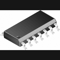
LMV824M National Semiconductor, LMV824M Datasheet - Page 12

LMV824M
Manufacturer Part Number
LMV824M
Description
Operational Amplifier (Op-Amp) IC
Manufacturer
National Semiconductor
Datasheet
1.LMV824M.pdf
(24 pages)
Specifications of LMV824M
No. Of Amplifiers
1
Bandwidth
5MHz
Slew Rate
2V/µs
No. Of Pins
14
Single Supply Voltage Min (+v)
2.7V
Amplifier Type
Operational
Mounting Type
Surface Mount
Peak Reflow Compatible (260 C)
No
Lead Free Status / RoHS Status
Contains lead / RoHS non-compliant
Available stocks
Company
Part Number
Manufacturer
Quantity
Price
Part Number:
LMV824M
Manufacturer:
NS/国半
Quantity:
20 000
Company:
Part Number:
LMV824MT
Manufacturer:
NS
Quantity:
4 162
Part Number:
LMV824MT
Manufacturer:
NS/国半
Quantity:
20 000
Company:
Part Number:
LMV824MTX
Manufacturer:
NS
Quantity:
61 000
Part Number:
LMV824MTX
Manufacturer:
NS/国半
Quantity:
20 000
Part Number:
LMV824MTX/NOPB
Manufacturer:
TI/德州仪器
Quantity:
20 000
Company:
Part Number:
LMV824MTX/NOPB
Manufacturer:
NS
Quantity:
15 047
Part Number:
LMV824MX
Manufacturer:
TI/德州仪器
Quantity:
20 000
www.national.com
1.3 Input Bias Current Consideration
Input bias current (I
offset voltage. This offset is primarily due to I
through the negative feedback resistor, R
is 90nA (max room) and R
will be developed (V
tor (R
input offset current (I
age in the same manner - typically 0.05 mV at room temp.
2.0 APPLICATION CIRCUITS
This section covers the following application circuits:
1. Telephone-Line Transceiver
2. “Simple” Mixer (Amplitude Modulator)
3. Dual Amplifier Active Filters (DAAFs)
5. Tri-level Voltage Detector
•
•
FIGURE 6. Canceling the Voltage Offset Effect of Input
C
a. Low-Pass Filter (LPF)
b. High-Pass Filter (HPF)
), as shown in Figure 6 , cancels out this affect. But the
FIGURE 5. Pulse Response per Figure 4
OS
B
OS
) can develop a somewhat significant
=I
Bias Current
) will still contribute to an offset volt-
B
x R
F
is 100 k , then an offset of 9 mV
F
).Using a compensation resis-
F
. For example, if I
DS100128-54
DS100128-59
B
flowing
B
12
2.1 Telephone-Line Transceiver
The telephone-line transceiver of Figure 7 provides a full-
duplexed connection through a PCMCIA, miniature trans-
former. The differential configuration of receiver portion
(UR), cancels reception from the transmitter portion (UT).
Note that the input signals for the differential configuration of
UR, are the transmit voltage (Vt) and Vt/2. This is because
R
ance; therefore dividing Vt by two (assuming R1
The differential configuration of UR has its resistors chosen
to cancel the Vt and Vt/2 inputs according to the following
equation:
Note that Cr is included for canceling out the inadequacies of
the lossy, miniature transformer. Refer to application note
AN-397 for detailed explanation.
2.2“Simple” Mixer (Amplitude Modulator)
The mixer of Figure 8 is simple and provides a unique form
of amplitude modulation. Vi is the modulation frequency
(F
carrier frequency (F
verting and non-inverting unity gain configurations. Offset-
ting a sine wave above ground at Vi results in the oscillo-
scope photo of Figure 9 .
The simple mixer can be applied to applications that utilize
the Doppler Effect to measure the velocity of an object. The
difference frequency is one of its output frequency compo-
nents. This difference frequency magnitude (/F
key factor for determining an object’s velocity per the Dop-
pler Effect. If a signal is transmitted to a moving object, the
reflected frequency will be a different frequency. This differ-
ence in transmit and receive frequency is directly propor-
tional to an object’s velocity.
match
FIGURE 7. Telephone-line Transceiver for a PCMCIA
M
), while a +3V square-wave at the gate of Q1, induces a
is chosen to match the coupled telephone-line imped-
C
). Q1 switches (toggles) U1 between in-
Modem Card
M
>>
DS100128-33
-F
C
R
/) is the
match
).


