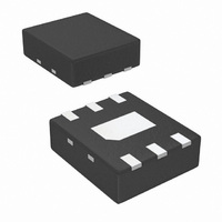
LM26LVCISD-105/NOPB National Semiconductor, LM26LVCISD-105/NOPB Datasheet - Page 16

LM26LVCISD-105/NOPB
Manufacturer Part Number
LM26LVCISD-105/NOPB
Description
IC TEMP SENS/SWITCH 105C 6LLP
Manufacturer
National Semiconductor
Series
PowerWise®r
Datasheet
1.LM26LVEB.pdf
(20 pages)
Specifications of LM26LVCISD-105/NOPB
Sensing Temperature
105°C Trip Point
Output Type
Active High/Push Pull, Active Low/Open Drain, Voltage
Voltage - Supply
1.6 V ~ 5.5 V
Accuracy
±2.2°C
Package / Case
6-WDFN Exposed Pad
Lead Free Status / RoHS Status
Lead free / RoHS Compliant
Other names
LM26LVCISD-105TR
www.national.com
4.3 VOLTAGE SHIFT
The LM26LV is very linear over temperature and supply volt-
age range. Due to the intrinsic behavior of an NMOS/PMOS
rail-to-rail buffer, a slight shift in the output can occur when
the supply voltage is ramped over the operating range of the
device. The location of the shift is determined by the relative
levels of V
V
This slight shift (a few millivolts) takes place over a wide
change (approximately 200 mV) in V
shift takes place over a wide temperature change of 5°C to
20°C, V
tions in the Electrical Characteristics table already includes
this possible shift.
DD
FIGURE 2. LM26LV with series resistor for capacitive
FIGURE 1. LM26LV No Decoupling Required for
− V
TEMP
TEMP
Capacitive Loads Less than 1100 pF.
DD
= 1.0V.
100 nF to 999 nF
is always monotonic. The accuracy specifica-
1.1 nF to 99 nF
loading greater than 1100 pF.
and V
C
1 μF
LOAD
TEMP
. The shift typically occurs when
Minimum R
DD
1.5 kΩ
800 Ω
3 kΩ
or V
TEMP
S
20204715
. Since the
20204733
16
5.0 Mounting and Temperature
Conductivity
The LM26LV can be applied easily in the same way as other
integrated-circuit temperature sensors. It can be glued or ce-
mented to a surface.
The best thermal conductivity between the device and the
PCB is achieved by soldering the DAP of the package to the
thermal pad on the PCB. The temperatures of the lands and
traces to the other leads of the LM26LV will also affect the
temperature reading.
Alternatively, the LM26LV can be mounted inside a sealed-
end metal tube, and can then be dipped into a bath or screwed
into a threaded hole in a tank. As with any IC, the LM26LV
and accompanying wiring and circuits must be kept insulated
and dry, to avoid leakage and corrosion. This is especially true
if the circuit may operate at cold temperatures where con-
densation can occur. If moisture creates a short circuit from
the V
LM26LV will not be correct. Printed-circuit coatings are often
used to ensure that moisture cannot corrode the leads or cir-
cuit traces.
The thermal resistance junction-to-ambient (θ
rameter used to calculate the rise of a device junction tem-
perature due to its power dissipation. The equation used to
calculate the rise in the LM26LV's die temperature is
where T
rent, I
voltage. For example, in an application where T
V
I
ing a self-heating error of only 0.021°C. Since the LM26LV's
junction temperature is the actual temperature being mea-
sured, care should be taken to minimize the load current that
the V
put is used with a 100 k pull-up resistor, and this output is
asserted (low), then for this example the additional contribu-
tion is [(152° C/W)x(5V)
heating error of 0.059°C.
resistance of the LM26LV.
L
DD
Device Number
= 2 μA, the junction temperature would be 30.021 °C, show-
LM26LVCISD
= 5 V, I
TEMP
TEMP
L
is the load current on the output, and V
A
FIGURE 3. LM26LV Thermal Resistance
is the ambient temperature, I
output to ground or V
output is required to drive. If The OVERTEMP out-
DD
= 9 μA, Gain 4, V
NS Package
2
SDB06A
/100k] = 0.038°C for a total self-
Number
Figure 3
DD
, the V
TEMP
Q
shows the thermal
TEMP
is the quiescent cur-
Resistance (θ
= 2231 mV, and
output from the
152° C/W
Thermal
O
JA
is the output
) is the pa-
A
= 30 °C,
JA
)


