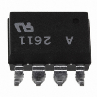
HCPL-2611#300 Avago Technologies US Inc., HCPL-2611#300 Datasheet - Page 10

HCPL-2611#300
Manufacturer Part Number
HCPL-2611#300
Description
OPTOCOUPLER, LOGIC GATE, 3750VRMS
Manufacturer
Avago Technologies US Inc.
Specifications of HCPL-2611#300
No. Of Channels
1
Optocoupler Output Type
Logic Gate
Input Current
15mA
Output Voltage
7V
Opto Case Style
SMD
No. Of Pins
8
Propagation Delay Low-high
100ns
Isolation Voltage
3.75kV
Voltage - Isolation
3750Vrms
Number Of Channels
1, Unidirectional
Current - Output / Channel
50mA
Data Rate
10MBd
Propagation Delay High - Low @ If
50ns @ 7.5mA
Current - Dc Forward (if)
20mA
Input Type
DC
Output Type
Open Collector
Mounting Type
Surface Mount, Gull Wing
Package / Case
8-SMD Gull Wing
Lead Free Status / RoHS Status
Contains lead / RoHS non-compliant
Other names
516-1079-5
Available stocks
Company
Part Number
Manufacturer
Quantity
Price
Propagation Delay,
Pulse-Width Distortion and Propagation Delay Skew
Propagation delay is a figure of merit which describes
how quickly a logic signal propagates through a sys-
tem. The propaga tion delay from low to high (t
amount of time required for an input signal to propagate
to the output, causing the output to change from low to
high. Similarly, the propagation delay from high to low
(t
nal to propagate to the output, causing the output to
change from high to low (see Figure 7).
Pulse-width distortion (PWD) results when t
differ in value. PWD is defined as the difference between
t
rate capability of a transmission system. PWD can be
expressed in percent by dividing the PWD (in ns) by the
minimum pulse width (in ns) being transmitted. Typi-
cally, PWD on the order of 20-30% of the minimum pulse
width is tolerable; the exact figure depends on the par-
ticular appli cation (RS232, RS422, T-1, etc.).
Propagation delay skew, t
eter to consider in parallel data appli cations where
synchroniza tion of signals on parallel data lines is a con-
cern. If the parallel data is being sent through a group
of optocouplers, differ ences in propagation delays will
cause the data to arrive at the outputs of the optocou-
plers at different times. If this difference in propagation
delays is large enough, it will determine the maximum
rate at which parallel data can be sent through the op-
tocouplers.
Propagation delay skew is defined as the difference be-
tween the minimum and maximum propagation delays,
either t
which are operating under the same conditions (i.e., the
same drive current, supply voltage, output load, and op-
erating tempera ture). As illustrated in Figure 15, if the in-
PLH
PHL
) is the amount of time required for the input sig-
and t
PLH
PHL
or t
and often determines the maxi mum data
PHL
, for any given group of optocouplers
PSK
, is an important param-
PLH
PLH
and t
) is the
PHL
puts of a group of optocouplers are switched either ON
or OFF at the same time, t
the shortest propagation delay, either t
the longest propaga tion delay, either t
As mentioned earlier, t
parallel data transmission rate. Figure 11 is the timing
diagram of a typical parallel data application with both
the clock and the data lines being sent through opto-
couplers. The figure shows data and clock signals at the
inputs and outputs of the optocouplers. To obtain the
maximum data transmission rate, both edges of the
clock signal are being used to clock the data; if only one
edge were used, the clock signal would need to be twice
as fast.
Propagation delay skew represents the uncertainty of
where an edge might be after being sent through an op-
tocoupler. Figure 16 shows that there will be uncertainty
in both the data and the clock lines. It is important that
these two areas of uncertainty not overlap, otherwise
the clock signal might arrive before all of the data out-
puts have settled, or some of the data outputs may start
to change before the clock signal has arrived. From these
considerations, the absolute minimum pulse width that
can be sent through optocouplers in a parallel applica-
tion is twice t
longer pulse width to ensure that any additional uncer-
tainty in the rest of the circuit does not cause a prob-
lem.
The t
guaranteed specifications for propagation delays, pulse-
width distortion and propagation delay skew over the
recommended temperature, and input current, and
power supply ranges.
PSK
specified optocouplers offer the advantages of
PSK
. A cautious design should use a slightly
PSK
can determine the maximum
PSK
is the difference between
PLH
PLH
or t
or t
PHL
PHL
.
, and


