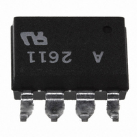
HCPL-2611#300 Avago Technologies US Inc., HCPL-2611#300 Datasheet - Page 4

HCPL-2611#300
Manufacturer Part Number
HCPL-2611#300
Description
OPTOCOUPLER, LOGIC GATE, 3750VRMS
Manufacturer
Avago Technologies US Inc.
Specifications of HCPL-2611#300
No. Of Channels
1
Optocoupler Output Type
Logic Gate
Input Current
15mA
Output Voltage
7V
Opto Case Style
SMD
No. Of Pins
8
Propagation Delay Low-high
100ns
Isolation Voltage
3.75kV
Voltage - Isolation
3750Vrms
Number Of Channels
1, Unidirectional
Current - Output / Channel
50mA
Data Rate
10MBd
Propagation Delay High - Low @ If
50ns @ 7.5mA
Current - Dc Forward (if)
20mA
Input Type
DC
Output Type
Open Collector
Mounting Type
Surface Mount, Gull Wing
Package / Case
8-SMD Gull Wing
Lead Free Status / RoHS Status
Contains lead / RoHS non-compliant
Other names
516-1079-5
Available stocks
Company
Part Number
Manufacturer
Quantity
Price
Insulation and Safety Related Specifications
IEC/EN/DIN EN 60747-5-5 Insulation Characteristics* (Option 060)
*
** Refer to the following figure for dependence of P
Recommended Operating Conditions
*
** The initial switching threshold is 5mA or less. It is recommended that 6.3mA to 10mA be used for best performance and to permit at least a
4
Parameter
Minimum External Air Gap
(External Clearance)
Minimum External
Tracking (External Creepage)
Minimum Internal Plastic Gap
(Internal Clearance)
Tracking Resistance
(Comparative Tracking Index)
Isolation Group
Description
Installation classification per DIN VDE 0110/39, Table 1
Climatic Classification
Pollution Degree (DIN VDE 0110/1.89)
Maximum Working Insulation Voltage
Input to Output Test Voltage, Method b*
V
Partial discharge < 5 pC
Input to Output Test Voltage, Method a*
V
Partial discharge < 5 pC
Highest Allowable Overvoltage
(Transient Overvoltage t
Safety-limiting values – maximum values allowed in the event
of a failure.
Insulation Resistance at T
Parameter
Input Current, Low Level
Input Current, High Level
Supply Voltage, Output
Fan Out (R
Output Pull-Up Resistor
Operating Temperature
IORM
IORM
for rated mains voltage
Refer to the optocoupler section of the Isolation and Control Components Designer’s Catalog, under Product Safety Regulations section, (IEC/
EN/DIN EN 60747-5-2) for a detailed description of Method a and Method b partial discharge test profiles.
The off condition can also be guaranteed by ensuring that V
20% LED degradation guardband.
for rated mains voltage
Case Temperature
Input Current**
Output Power**
x 1.875=V
x 1.5=V
L
= 1 kΩ)
PR
, Type and Sample Test, tm=60 sec,
PR
, 100% Production Test with tm=1 sec,
ini
S
d
, V
d
=10 sec)
300 Vrms
IO
150 Vrms
= 500 V
Symbol
I
I
V
N
R
T
FL
FH
CC
A
L
*
**
Symbol
L(101)
L(102)
CTI
S
Min.
0
5
4.5
330
-40
and I
Value
5
5
0.08
175
IIIa
S
on ambient temperature.
F
(off ) ≤ 0.8 volts.
Max.
250
15
5.5
5
4,000
85
Units
mm
mm
mm
V
Symbol
V
V
V
V
T
I
P
R
S, INPUT
S
IORM
PR
PR
IOTM
S, OUTPUT
S
Units
μA
mA
V
TTL Loads
Ω
°C
Conditions
Measured from input terminals to output terminals,
shortest distance through air.
Measured from input terminals to output terminals,
shortest distance path along body.
Through insulation distance conductor to conductor,
usually the straight line distance thickness between
the emitter and detector.
DIN IEC 112/VDE 0303 Part 1
Material Group (DIN VDE 0110, 1/89, Table 1)
Characteristic
I – IV
I – III
55/85/21
2
560
1050
840
6000
150
150
600
>10
9
Unit
Vpeak
Vpeak
Vpeak
Vpeak
°C
mA
mW
:


