CRD-5376 Cirrus Logic Inc, CRD-5376 Datasheet
CRD-5376
Specifications of CRD-5376


Related parts for CRD-5376


CRD-5376 Summary of contents
Page 1
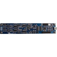
... Time domain analysis – Noise histogram analysis www.cirrus.com General Description The CRD5376 board is a reference design for the Cirrus Logic multichannel seismic chip set. Data sheets for the CS3301A, CS3302A, CS4373A, CS5371A/72A, and CS5376A devices should be consulted when using the CRD5376 reference design ...
Page 2
... Intel and Pentium are registered trademarks of Intel Corporation. USBXpress is a registered trademark of Silicon Laboratories, Inc. SPI is a trademark of Motorola, Inc. Microwire is a trademark of National Semiconductor Corporation registered trademark of Philips Semiconductor Initial Release. BOM change to latest revision of silicon. Minor layout enhancements. www.cirrus.com CRD5376 Changes DS612RD2 ...
Page 3
... Default Jumper Settings ........................................................................................ 6 1.3 Software Setup .................................................................................................................. 7 1.3.1 PC Requirements .................................................................................................. 7 1.3.2 Seismic Evaluation Software Installation .............................................................. 7 1.3.3 USBXpress Driver Installation ............................................................................... 7 1.3.4 Launching the Seismic Evaluation Software ......................................................... 8 1.4 Self-Testing CRD5376 ....................................................................................................... 9 1.4.1 Noise Test ............................................................................................................. 9 1.4.2 Distortion Test ..................................................................................................... 10 2. HARDWARE DESCRIPTION ................................................................................................. 11 2.1 Block Diagram ................................................................................................................ 11 2.2 Analog Hardware ............................................................................................................. 12 2 ...
Page 4
... GPIO ................................................................................................................... 47 3.5.6 Customize ........................................................................................................... 48 3.5.7 External Macros .................................................................................................. 48 4. BILL OF MATERIALS ........................................................................................................... 49 5. LAYER PLOTS ...................................................................................................................... 51 6. SCHEMATICS ........................................................................................................................ 57 Figure 1. CRD5376 Block Diagram ............................................................................................... 11 Figure 2. Differential Pair Routing ................................................................................................. 30 Figure 3. Quad Group Routing ...................................................................................................... 30 Figure 4. Bypass Capacitor Placement ......................................................................................... 31 Table 1. Amplifier Pin 13 Jumper Settings ...................................................................................... 6 Table 2. SDTKI Input Jumper Settings............................................................................................ 6 Table 3 ...
Page 5
... With power off, connect the CRD5376 power inputs to the power supply outputs. J8 pin pin pin pin • Connect the USB cable between the CRD5376 USB connector and the PC USB port. • Proceed to the Software Setup section to install the evaluation software and USB driver. DS612RD2 CRD5376 5 ...
Page 6
... Default Jumper Settings * indicates the default jumper installation for CRD5376. CH1 CH2 CH3 CH4 Table 1. Amplifier Pin 13 Jumper Settings SDTKI Table 3. PLL Clock Input Jumper Settings 6 Amplifier CS3301A U16 *R128 + *R84 U2 *R86 + *R92 U33 R95 + R132 U3 R58 + R100 CS5376A uController ...
Page 7
... Silicon Laboratories (http://www.silabs.com). For convenience, the USBXpress driver files are included as part of the installation package. To install the USBXpress driver (after installing the Seismic Evaluation Software): • Connect CRD5376 to the PC through an available USB port and apply power. The PC will detect DS612RD2 CRD5376 ® ...
Page 8
... Files\Cirrus Seismic Evaluation\Driver\”. The PC will recognize and install the USBXpress device driver. • After driver installation, cycle power to CRD5376. The PC will automatically detect it and add USBXpress device in the Windows Hardware Device Manager. An application note, AN271 - Cirrus Seismic Evaluation GUI Installation Guide, is available from the Cirrus Logic web site with step-by-step instructions on installing the USBXpress driver ...
Page 9
... Noise and distortion self-tests can be performed once hardware and software setup is complete. First, initialize the CRD5376 reference design: • Launch the evaluation software and apply power to CRD5376. • Click ‘OK’ on the About panel to get to the Setup panel. • On the Setup panel, select Open Target on the USB Port sub-panel. ...
Page 10
... After digital filter configuration is complete, click Capture on the Data Capture sub-panel. • Once the data record is collected, the Analysis panel is automatically displayed. • Select Signal FFT from the Test Select control to display the calculated noise statistics. • Verify the distortion performance (S/D) is 112 dB or better. 10 CRD5376 DS612RD2 ...
Page 11
... HARDWARE DESCRIPTION 2.1 Block Diagram Major blocks of the CRD5376 reference design include: • CS3301A Geophone Amplifier (2x) • CS3302A Hydrophone Amplifier (2x) • CS5372A Dual ∆Σ Modulators (2x) • CS5376A Digital Filter • CS4373A ∆Σ Test DAC • Analog Switch Multiplexer • Precision Voltage Reference • ...
Page 12
... Other sensors for earthquake monitoring and military applications are considered as geophones for this datasheet. External signals connect to CRD5376 through 3-pin headers on the left side of the PCB. For each channel (CH1, CH2, CH3, CH4), these headers make connections to the differential INA amplifier inputs and to either a GND or GUARD signal for connection to the sensor cable shields, if present ...
Page 13
... The small physical size of these ESD diodes restricts their current capacity to 10 mA. For land applications using the CS3301A amplifier (CRD5376 channels 1 and 2), the INA input has a com- mon-mode and differential-mode RC filter. The common-mode filter sets a low-pass corner to shunt very high frequency components to ground with minimal noise contribution ...
Page 14
... Resistors to create the common mode bias are selected based on the sensor impedance and may need to be modified from the CRD5376 defaults depending on the sensor to be used. Refer to the recommended operating bias conditions for the selected sensor, which are available from the sensor manufacturer ...
Page 15
... Channel 4 Only 100 Even Channels Connected 101 Odd Channels Connected 110 All Channels Connected 111 All Channels Disconnected Table 5. Analog Switch Settings CRD5376 Value CD74HC4051PWR TSSOP-16 +3.3V, 160 µA 000, 001, 010, 011 100, 101 110 111 Value SN74LVC2G32DCTR SSOP-8 +2 µ ...
Page 16
... MCLK/2 Input vs. GUARD Output By default, channels 1 and 2 of CRD5376 use the CS3301A geophone amplifier while channels 3 and 4 use the CS3302A hydrophone amplifier. The CS3301A amplifier is chopper stabilized and connects pin clock source (MCLK/2) to run the chopper circuitry synchronous to the modulator analog sampling clock ...
Page 17
... RC filters are required between the CS3301A/02A amplifier outputs and the CS5372A modulator inputs to bandwidth limit analog signals into the modulator. For the CRD5376, the CS3301A/02A amplifier outputs are connected to external 680 Ω series resistors, and a differential anti-alias RC filter is created by connecting high linearity differential capacitance ( C0G) between each half of the rough and fine signals ...
Page 18
... Voltage Reference A voltage reference on CRD5376 creates a precision voltage from the regulated analog supplies for the modulator and test DAC VREF inputs. Because the voltage reference output is generated relative to the negative analog power supply, VREF+ is near GND potential for bipolar power supplies. ...
Page 19
... Master clock input, 32.768 MHz Master synchronization input, rising edge triggered Description Serial chip select input, active low Serial clock input Master in / slave out serial data Master out / slave in serial data Serial acknowledge output, active low Serial chip select output (unused on CRD5376) CRD5376 19 ...
Page 20
... Modulator clock output, half-speed Modulator synchronization output Modulator delta-sigma data inputs Modulator over-range flag inputs Test DAC delta-sigma data output Test DAC clock output (unused on CRD5376) Description Amplifier input mux selection Amplifier gain / test DAC attenuation Test DAC mode selection Amplifier / modulator power down ...
Page 21
... How the digital filter receives configuration information, either from a microcontroller or configuration EE- PROM, is selected by the BOOT signal. The BOOT signal is tied low on CRD5376 for microcontroller configuration. 2.3.1.3 ...
Page 22
... CRD5376 input from the microcontroller to initiate data transactions on command or from the MCLK/2 clock to initiate data transactions automatically as soon as they are available from the digital filter. CS5376A SDTKI 2.3.2 Microcontroller Included on CRD5376 is an 8051-type microcontroller with integrated hardware SPI and USB interfaces. ...
Page 23
... C8051F320 has dedicated pins for power and the USB connection, plus 25 general purpose I/O pins that connect to the various internal resources through a programmable crossbar. Hardware connections on CRD5376 limit how the blocks can operate, so the port mapping of microcontroller resources is detailed below. Pin # ...
Page 24
... SPI chip select output, active low SPI master out / slave in SPI master in / slave out SPI serial clock Internal VREF bypass capacitors Serial acknowledge from CS5376A, active low UART receiver UART transmitter External clock input Data ready acknowledge from CS5376A, active low CRD5376 DS612RD2 ...
Page 25
... Detector Architecture The expected input clock frequency to the external connector is set by jumper options external clock is supplied to CRD5376, the PLL will free-run at the nominal output frequency. A jumper option is available to output the clock to the external connector, making it the system clock source. Input Clock 1 ...
Page 26
... The PLL on CRD5376 uses a voltage controlled crystal oscillator (VCXO) to minimize jitter, and has a sin- gle gate phase/frequency detector and clock divider to minimize size and power. Specification Oscillator - Citizen 32.768 MHz VCXO Surface Mount Package Type Supply Voltage, Current Frequency Stability, Pullability ...
Page 27
... Specification I2C Inputs, 2 wires each I2C Outputs, 2 wires each I2C Bypass Switch Control When CRD5376 is used in a distributed measurement network, each node must have a unique address. This address is used to transmit individual configuration commands and tag the source of returned con- DS612RD2 CRD5376 Value CLK± ...
Page 28
... Power Supplies Power is supplied to CRD5376 through the +3.3 V and -3.3 V voltage inputs on the external connector (J8), which are typically from an external AC-DC or DC-DC converter. Digital circuitry on CRD5376 is driv- en directly from the +3.3 V input, while linear regulators create +2.5 V and - 2.5 V analog power supplies from +3 ...
Page 29
... Analog Voltage Regulators Linear voltage regulators create the positive and negative analog power supply voltages to the analog components on CRD5376. These regulate the +3.3 V and -3.3 V power supply inputs to create the +2.5 V and -2.5 V analog power supplies. Specification Positive Analog Power Supply ...
Page 30
... CRD5376 layer solid ground plane without splits or routing. A solid ground plane provides the best return path for bypassed noise to leave the system. No separate analog ground is required since analog signals on CRD5376 are differentially routed. CRD5376 layer 6 is dedicated for analog and digital routing. Critical analog signal routes for channels 3 and 4 are on this layer ...
Page 31
... Each device power supply pin includes 0.1 µF bypass capacitors placed as close as possible to the pin. Each power supply net includes at least 100 µF bulk capacitance as a charge well for transient current loads. VA+ bypass DS612RD2 VD bypass CS3301A Device Figure 4. Bypass Capacitor Placement CRD5376 VA- bypass 31 ...
Page 32
... Prints using the standard resolution of the screen. Exits the application software. Displays the Setup Panel. Displays the Analysis Panel. Displays the Control Panel. Displays the Setup Panel and starts Data Capture. Find help by topic. Find help by keywords. Displays the About Panel. CRD5376 DS612RD2 ...
Page 33
... About Panel The About panel displays copyright information for the Cirrus Seismic Evaluation software. Click OK to exit this panel. Select Help DS612RD2 About from the menu bar to display this panel. CRD5376 33 ...
Page 34
... Setup Panel The Setup panel initializes the evaluation system to perform data acquisition. It consists of the following sub-panels and controls. • USB Port • Digital Filter • Analog Front End • Test Bit Stream • Gain/Offset • Data Capture • External Macros 34 CRD5376 DS612RD2 ...
Page 35
... Programs the microcontroller code on the target board using the .thx file found in the “C:\Program Files\Cirrus Seismic Evaluation” directory. This feature permits repro- gramming of the microcontroller (without using a hardware programmer) when a new version of the MCU code becomes available. DS612RD2 Description CRD5376 35 ...
Page 36
... Sets the analog sample clock rate. The CS5372A modulators and CS4373A test DAC typically run with MCLK set to 2.048 MHz. Configure Writes all information from the Setup panel to the digital filter. The data Capture but- ton becomes available once the configuration information is written to the target board. 36 Description CRD5376 DS612RD2 ...
Page 37
... Manual control for the output clock and data rate of the test bit stream generator. Gain Factor Manual control to set the test bit stream signal amplitude. Sync Enables test bit stream synchronization by the MSYNC signal. Loopback Enables digital loopback from the test bit stream generator output to the digital filter input. DS612RD2 Description Description CRD5376 37 ...
Page 38
... Enables offset correction. When enabled, output samples are offset by the value in the OFFSET register. (Output = Sample - OFFSET). ORCAL Enables offset calibration using the exponent value from the EXP[4:0] control. Results are automatically written to the OFFSET registers as they are calculated. EXP[4:0] Sets the exponential value used by offset calibration. 38 Description CRD5376 DS612RD2 ...
Page 39
... Indicates how many more data captures are remaining to complete the requested number of Total Captures. A zero value means that the current data capture is the last one. Skip Samples Sets the total number of samples to be skipped prior to data collection. A maximum of 64K samples can be skipped DS612RD2 Description CRD5376 39 ...
Page 40
... Control panel. These External Macros operate independently of the Macros sub- panel and are not affected by operations within it, except when a macro is saved to the . /macros/ subdi- rectory to replace a currently existing External Macro. Control Runs the External Macro associated with that button. 40 Description CRD5376 DS612RD2 ...
Page 41
... Analysis Panel The Analysis panel is used to display the analysis results on collected data. It consists of the following controls. • Test Select • Statistics • Plot Enable • Cursor • Zoom • Refresh • Harmonics • Spot Noise • Plot Error DS612RD2 CRD5376 41 ...
Page 42
... Statistics are calculated using the largest frequency bin as a full-scale signal reference. Noise FFT Runs an FFT on the collected data set and then plots frequency magnitude vs. fre- quency. Statistics are calculated using a simulated full-scale signal as a full-scale sig- nal reference. 42 Description CRD5376 DS612RD2 ...
Page 43
... Signal to Distortion of calculated FFT. Signal to Noise plus Distortion of calculated FFT. Number of Bins covering the Nyquist frequency. Signal to Noise of calculated FFT. Signal to Peak Noise of calculated FFT. Spot Noise in dB/Hz of calculated FFT. Spot Noise in nV/rtHz of calculated FFT. Number of Bins covering the Nyquist frequency. CRD5376 43 ...
Page 44
... Once an error code is displayed in the numerical box, a description can be displayed by clicking the PLOT ERROR button. This causes a dialog box to display showing the error number, the error channel, and a text error message. 44 CRD5376 DS612RD2 ...
Page 45
... Control Panel The Control panel is used to write and read register settings and to send commands to the digital filter. It consists of the following sub-panels and controls. • DF Registers • DF Commands • SPI1 • Macros • GPIO • Customize • External Macros DS612RD2 CRD5376 45 ...
Page 46
... Contains the third data word written to or read from the SPI registers. Read 1 Word Initiates a 1 word SPI read transaction. Read 3 Words Initiates a 3 word SPI read transaction. Write 1 Word Initiates a 1 word SPI write transaction. Write 3 Words Initiates a 3 word SPI write transaction. 46 Description Description Description CRD5376 DS612RD2 ...
Page 47
... Initiates a write to GPIO registers.The Direction, Pull Up and Data controls are read to determine the register values to be written. Read Initiates a read from GPIO registers.The Direction, Pull Up and Data controls are updated based on the register values that are read. DS612RD2 Description Description CRD5376 47 ...
Page 48
... Enables the digital filter by sending the Start Filter command. Stop Filter Disables the digital filter by sending the Stop Filter command. Write EEPROM Writes an EEPROM boot configuration file to EEPROM memory (unused on CRD5376A). Verify EEPROM Verifies EEPROM memory against an EEPROM boot configuration file (unused on CRD5376A) 3.5.7 External Macros Macros are generated within the Macros sub-panel on the Control panel ...
Page 49
... BILL OF MATERIALS DS612RD2 CRD5376 49 ...
Page 50
... CRD5376 DS612RD2 ...
Page 51
... LAYER PLOTS DS612RD2 CRD5376 51 ...
Page 52
... CRD5376 DS612RD2 ...
Page 53
... DS612RD2 CRD5376 53 ...
Page 54
... CRD5376 DS612RD2 ...
Page 55
... DS612RD2 CRD5376 55 ...
Page 56
... CRD5376 DS612RD2 ...
Page 57
... SCHEMATICS DS612RD2 CRD5376 57 ...
Page 58
... CRD5376 DS612RD2 ...
Page 59
... DS612RD2 CRD5376 59 ...
Page 60
... CRD5376 DS612RD2 ...
Page 61
... DS612RD2 CRD5376 61 ...
Page 62
... CRD5376 DS612RD2 ...
Page 63
... DS612RD2 CRD5376 63 ...
Page 64
... CRD5376 DS612RD2 ...
Page 65
... DS612RD2 CRD5376 65 ...
Page 66
... CRD5376 DS612RD2 ...
Page 67
... DS612RD2 CRD5376 67 ...
Page 68
... CRD5376 DS612RD2 ...