RO3101A RFM, RO3101A Datasheet - Page 2
RO3101A
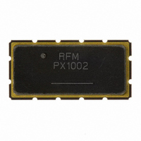
Manufacturer Part Number
RO3101A
Description
RESONATOR, SM5035-4
Manufacturer
RFM
Series
RO3101Ar
Type
SAWr
Datasheet
1.RO3101A.pdf
(2 pages)
Specifications of RO3101A
Frequency
433.92MHz
Features
without Capacitor
Frequency Stability
±0.032ppm
Frequency Tolerance
±75kHz
Operating Temperature
-40°C ~ 85°C
Mounting Type
Surface Mount
Package / Case
4-SMD
Size / Dimension
0.197" L x 0.138" W (5.00mm x 3.50mm)
Height
0.060" (1.53mm)
Lead Free Status / RoHS Status
Lead free / RoHS Compliant
Other names
583-1071-2
Available stocks
Company
Part Number
Manufacturer
Quantity
Price
Company:

Part Number:
RO3101A
Manufacturer:
RFMD
Quantity:
5 000
Company:
Part Number:
RO3101A-1
Manufacturer:
RFMD
Quantity:
5 000
Company:
Part Number:
RO3101A-11
Manufacturer:
RFMD
Quantity:
5 000
Company:
Part Number:
RO3101A-14
Manufacturer:
RFMD
Quantity:
5 000
Company:
Part Number:
RO3101A-21
Manufacturer:
RFMD
Quantity:
5 000


Electrical Connections
The SAW resonator is bidirectional and may be
installed with either orientation. The two terminals
are interchangeable and unnumbered. The callout
NC indicates no internal connection. The NC pads
assist with mechanical positioning and stability.
External grounding of the NC pads is
recommended to help reduce parasitic
capacitance in the circuit.
Typical Test Circuit
The test circuit inductor, L
capacitance, C
Typical Application Circuits
www.RFM.com
©2008 by RF Monolithics, Inc.
Modulation
RO3XXXA
Bottom View
RO3XXXA
Bottom View
Typical Low-Power Transmitter Application
Typical Local Oscillator Applications
POWER TEST
ELECTRICAL TEST
50 Ω Source
at F
CW RF Power Dissipation =
+VDC
C
Input
O
, at F
From 50 Ω
Network Analyzer
E-mail: info@rfm.com
200k Ω
P
P
REFLECTED
INCIDENT
C
.
TEST
, is tuned to resonate with the static
Low-Loss
Matching
Network to
50 Ω
C1
P
INCIDENT -
470
C2
C1
C2
P
REFLECTED
(Antenna)
L1
NC
RF Bypass
RF Bypass
To 50 Ω
Network Analyzer
L1
+9VDC
Output
Terminal
Terminal
+VDC
Terminal
Terminal
NC
47
Equivalent LC Mode
Temperature Characteristics
The curve shown on the right
accounts for resonator
contribution only and does not
include LC component
temperature contributions.
Typical
Land Pattern
The circuit board land pattern
shown below is one possible
design. The optimum land pattern is dependent on the circuit board
assembly process which varies by manufacturer. The distance between
adjacent land edges should be at a maximum to minimize parasitic
capacitance. Trace lengths from terminal lands to other components should
be short and wide to minimize parasitic series inductances.
Case Design
Dimensions
G
A
B
C
D
E
F
Top View
Circuit
B
Min
4.87
3.37
1.45
1.35
1.07
.67
.37
Board
Millimeters
Rm
Nom
1.53
1.43
1.20
l
5.0
3.5
.80
.50
Lm
Side View
(4 Places)
Typical Dimension:
0.010 to 0.047 inch
(0.25 to 1.20 mm)
0.05 pF*
C p
C
D
Cm
-150
-200
-100
Max
-50
5.13
3.63
1.60
1.50
1.33
.93
.63
0
-80 -60 -40 -20
Δ T = T
C o
Min
.191
.132
.057
.040
.026
.014
.042
=
Bottom View
C p
*Case Parasitics
C
3
+
- T
0 +20 +40 +60
0.05 pF
O
Inches
4
2
f
( °C )
Nom
C
RO3101A - 3/26/08
.196
.137
.060
.057
.031
.019
.047
= f
1
O
, T
Page 2 of 2
C
+80
= T
Max
0
-50
-100
-150
-200
E (3x)
F (4x)
.201
.142
.062
.059
.036
.024
.052
G (1x)
O
Related parts for RO3101A
Image
Part Number
Description
Manufacturer
Datasheet
Request
R

Part Number:
Description:
ASH RX 115.2 KBPS 433.92 MHZ
Manufacturer:
RFM
Datasheet:

Part Number:
Description:
RFIC TRANCEIVER MULTI-CHANNEL FS
Manufacturer:
RFM
Datasheet:

Part Number:
Description:
ASH TX 115.2 KBPS 433.92 MHZ
Manufacturer:
RFM
Datasheet:
Part Number:
Description:
Filters 1602MHz BW=61MHz
Manufacturer:
RFM
Datasheet:

Part Number:
Description:
RESONATOR, SM3030-6
Manufacturer:
RFM
Datasheet:

Part Number:
Description:
RESONATOR, SM3030-6
Manufacturer:
RFM
Datasheet:

Part Number:
Description:
RESONATOR, SM3030-6
Manufacturer:
RFM
Datasheet:
Part Number:
Description:
RESONATOR 418MHZ SM5035-4
Manufacturer:
RFM
Datasheet:
Part Number:
Description:
RESONATOR 315 MHZ SMD
Manufacturer:
RFM
Datasheet:

Part Number:
Description:
RESONATOR, SM5035-4
Manufacturer:
RFM
Datasheet:

Part Number:
Description:
10-Terminal Ceramic Surface-Mount Case 7 x 5 mm Nominal Footprint
Manufacturer:
RFM [RF Monolithics, Inc]
Datasheet:
Part Number:
Description:
QUAD-BAND GSM850/GSM/DCS/PCS POWER AMP MODULE
Manufacturer:
RFM [RF Monolithics, Inc]
Datasheet:
Part Number:
Description:
402 to 405 MHz Medical Band Front-end Filter
Manufacturer:
RFM [RF Monolithics, Inc]
Datasheet:
Part Number:
Description:
674.03 MHz SAW Resonator
Manufacturer:
RFM [RF Monolithics, Inc]
Datasheet: